Light field image capture device and image sensor

a technology of image capture device and image sensor, which is applied in the field of single-lens 3d image capture technology, can solve the problems of increasing not only the overall size of the image capture device, but also the manufacturing cost, and achieve the effect of reducing resolution

Active Publication Date: 2016-10-04
PANASONIC INTELLECTUAL PROPERTY MANAGEMENT CO LTD
View PDF32 Cites 0 Cited by
  • Summary
  • Abstract
  • Description
  • Claims
  • Application Information

AI Technical Summary

Benefits of technology

[0021]According to an aspect of the present invention, an image with no decrease in resolution and depth information can be obtained at the same time.

Problems solved by technology

According to such a so-called “two-lens image capturing” technique, however, two cameras need to be used, thus increasing not only the overall size of the image capture device but also the manufacturing cost as well.

Method used


Image

  • Light field image capture device and image sensor
  • Light field image capture device and image sensor
  • Light field image capture device and image sensor

Examples


embodiment 1

[0035](Embodiment 1)

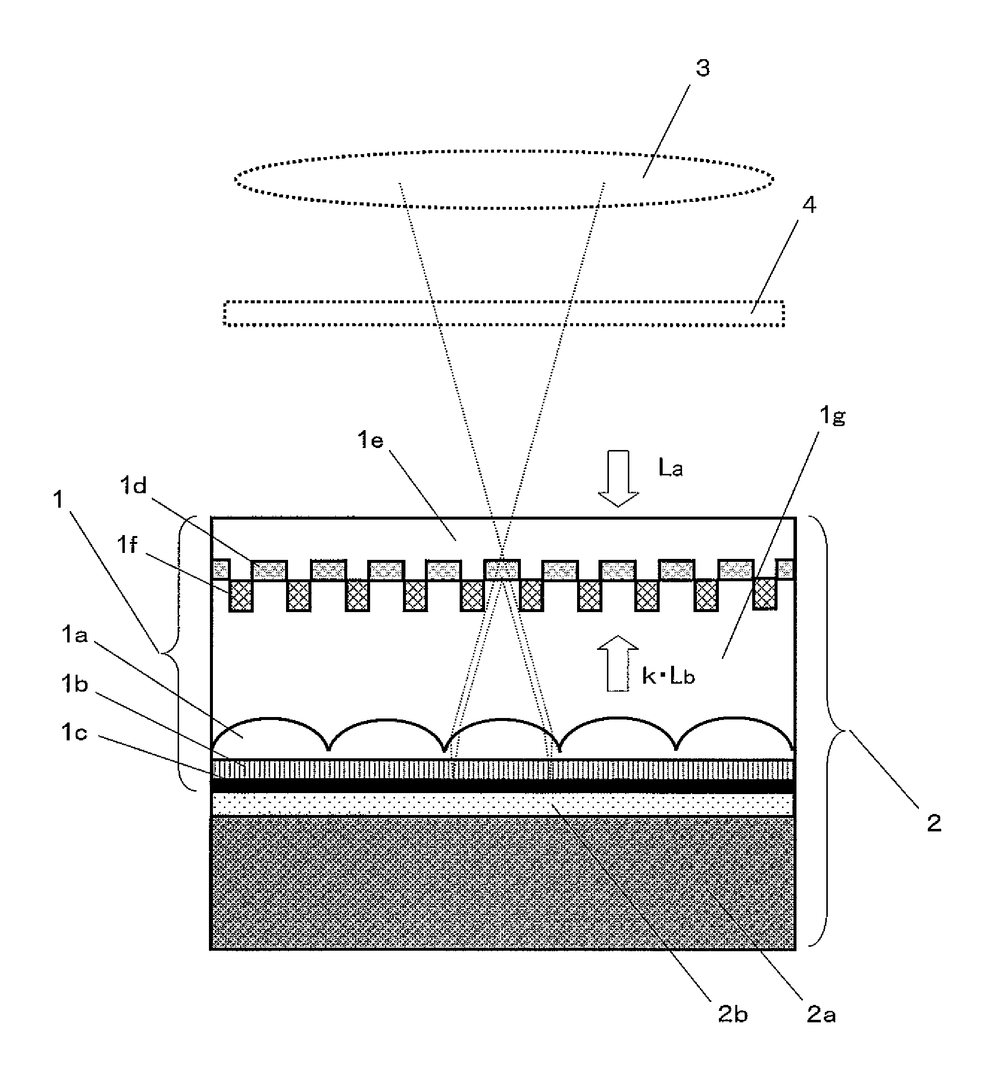
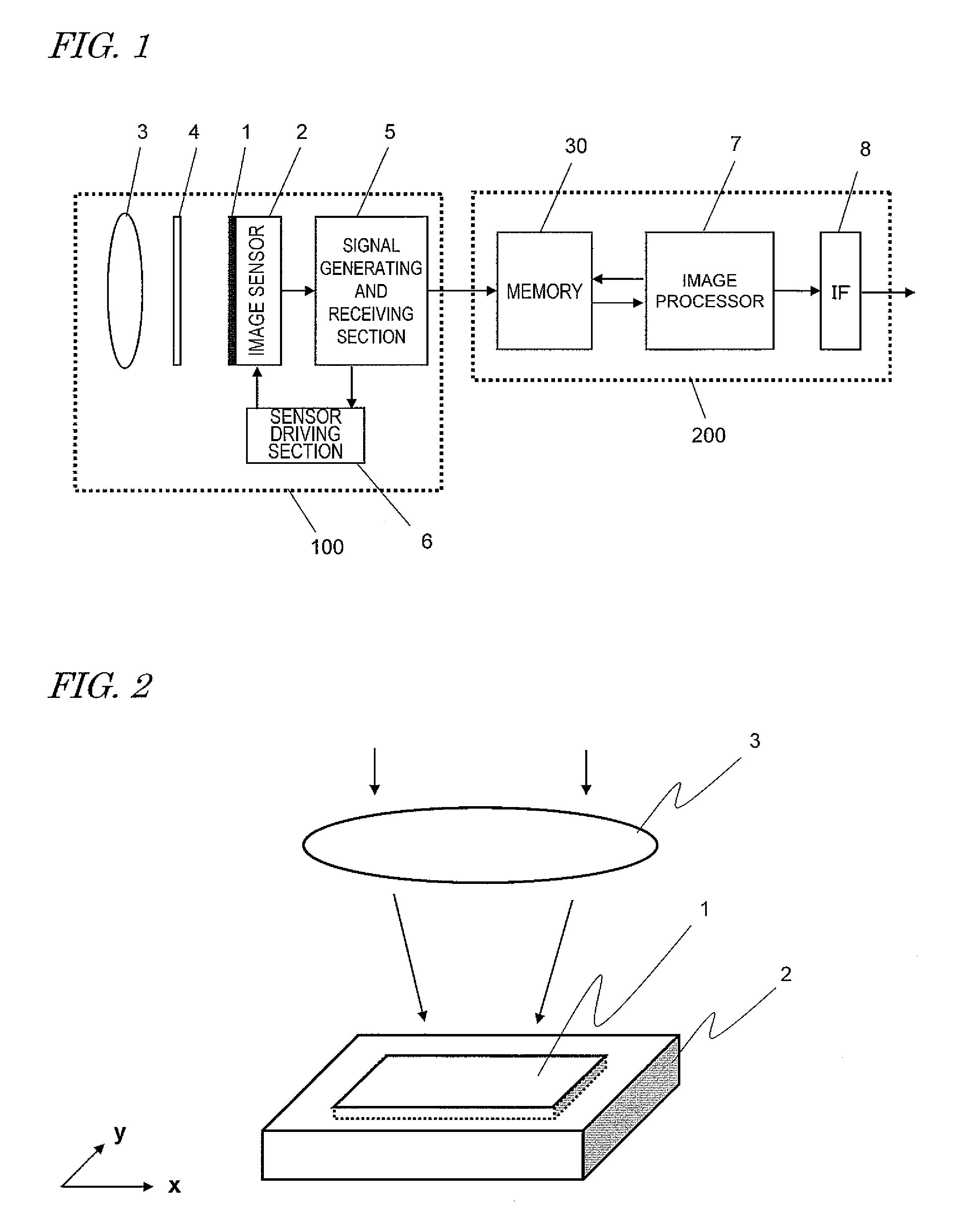
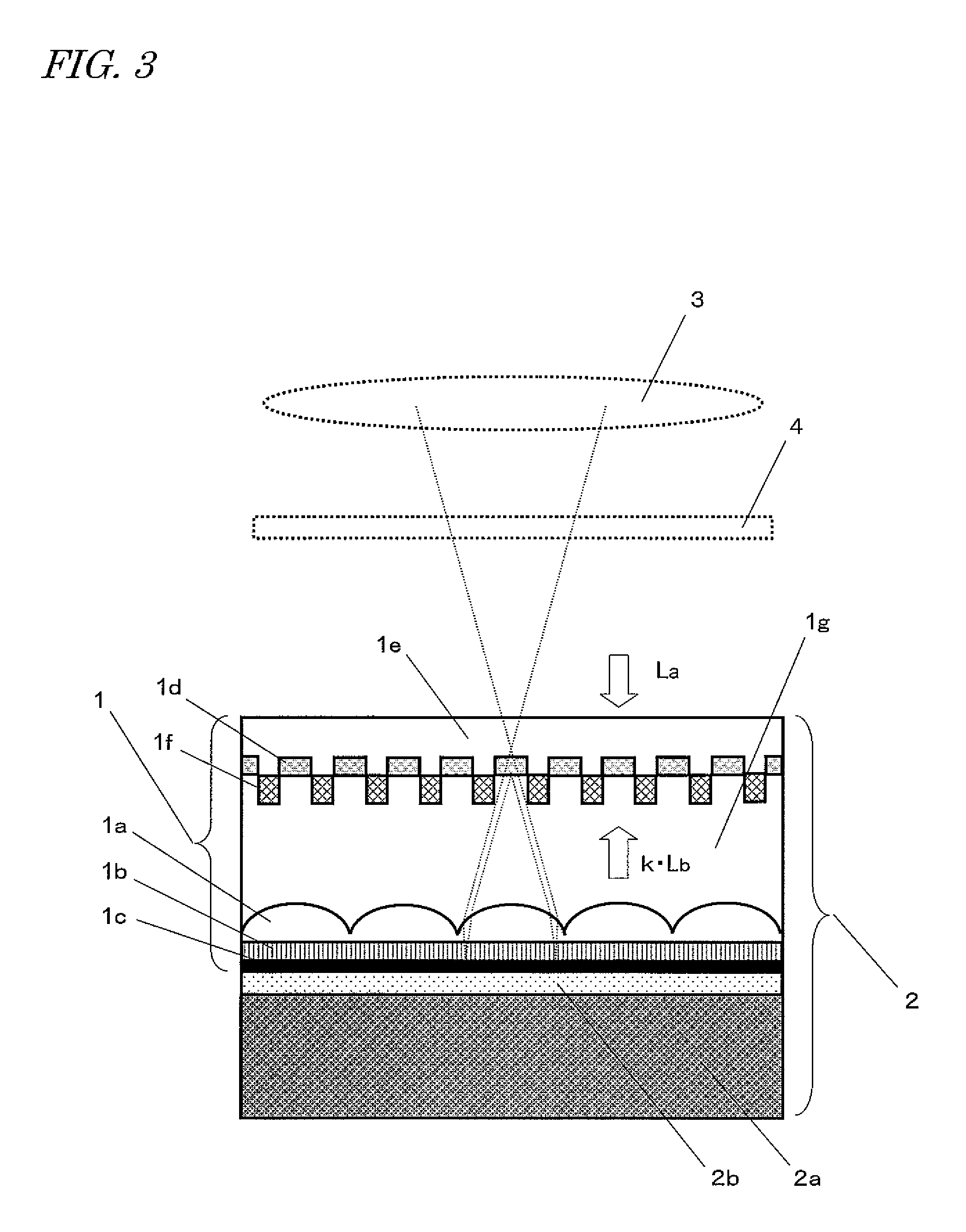
[0036]First of all, an image capture device as a first embodiment of the present invention will be described. FIG. 1 is a block diagram illustrating a general configuration for a light field image capture device according to this embodiment (which will be simply referred to herein as an “image capture device”). The image capture device of this embodiment is a digital electronic camera and includes an image capturing section 100 and a signal processing section 200 that generates a signal representing an image (i.e., an image signal) based on the signal generated by the image capturing section 100.

[0037]The image capturing section 100 includes a solid-state image sensor 2 (which will be simply referred to herein as an “image sensor”) with a number of photosensitive cells that are arranged on its imaging area, an optical lens 3 (imaging section) which produces an image on the photoelectric conversion section 1 of the image sensor 2, and an infrared cut filter 4. The...


PUM


Abstract

An image sensor 2 includes: a photoelectric conversion layer 1d including a plurality of photosensitive cells; a reflective layer 1c that reflects light that has been transmitted through the photoelectric conversion layer 1d; a micro lens layer 1a that includes a plurality of micro lenses that are arranged between the photoelectric conversion layer 1d and the reflective layer 1c; and a transmitted light controlling layer 1b that is arranged between the photoelectric conversion layer 1d and the reflective layer 1c and that is able to change optical transmittance in accordance with an instruction given by a controller. The micro lens layer 1a is arranged so that light that has been transmitted through one of the photosensitive cells and then reflected from the reflective layer 1c is incident on the same photosensitive cell again.

Description

TECHNICAL FIELD[0001]The present application relates to a single-lens 3D image capturing technology for obtaining an image and depth information at the same time.BACKGROUND ART[0002]Recently, the performance and functionality of digital cameras and digital movie cameras that use some solid-state image sensor such as a CCD or a CMOS (which will be sometimes simply referred to herein as an “image sensor”) have been enhanced to an astonishing degree. In particular, the size of a pixel structure for use in an image sensor has been further reduced these days thanks to rapid development of semiconductor device processing technologies, thus getting an even greater number of pixels and drivers integrated together in an image sensor. As a result, the resolution of an image sensor has lately increased rapidly from around one million pixels to ten million or more pixels in a matter of few years. On top of that, the quality of an image captured has also been improved significantly as well. As f...

Claims


Application Information

Patent Timeline
Patent Type & Authority Patents(United States)
IPC IPC(8): H04N13/02H01L27/146H04N5/374
CPCH04N13/021H01L27/1464H01L27/14627H01L27/14629H04N5/374H04N25/76H04N13/211
Inventor HIRAMOTO, MASAOISHII, YASUNORIMONOBE, YUSUKE
Owner PANASONIC INTELLECTUAL PROPERTY MANAGEMENT CO LTD
Why Eureka
Try Eureka