Display device configured to perform pseudo interlace scanning image display based on progressive image signal, driving method thereof, and display driving circuit

a display device and progressive image technology, applied in the direction of instruments, computing, electric digital data processing, etc., can solve the problems of shortened securable charge time, deterioration of substantial resolution of still image display, and flickering or blurring of edge portions of display images, so as to prevent flickering, high display performance, and resolution. deterioration

Inactive Publication Date: 2016-10-25
SHARP KK
View PDF21 Cites 0 Cited by
  • Summary
  • Abstract
  • Description
  • Claims
  • Application Information

AI Technical Summary

Benefits of technology

[0030]According to the first aspect of the present invention, with the pixel formation units, a display frame period which is a frame period for forming a pixel of an image to be displayed, and a black frame period which is a frame period for forming a black pixel alternately appear (black insertion for interlace is performed), and accordingly, even when optical response of each pixel formation unit is slow, video crosstalk from the previous frame is suppressed. Also, an arrangement is made wherein black display lines are formed every other scanning line in the pixel array by black insertion for interlace, and accordingly, occurrence of flickers can be prevented without increasing the frame frequency. Also, of two adjacent frames, with one of the frames, black insertion is performed on odd-numbered scanning lines, and with the other frame, black insertion is performed on even-numbered scanning lines, and accordingly, in the event of displaying a still image, a high-definition image is configured of images of two adjacent frames, and resolution does not deteriorate due to the black insertion for interlace. Accordingly, high display performance is obtained regarding both of moving images and still images even if definition of display images or increase in the size of display panels advance. Note that, in the event that the display device according to the first aspect of the present invention is a liquid crystal display device, insufficient charging of pixel capacitance at each pixel formation unit is prevented by the black insertion for interlace, and accordingly, this point also contributes to suitable display of a high-definition moving image.
[0031]According to the second aspect of the present invention, a black display line in the black insertion for interlace is displayed with lower luminance than 10% of the maximum luminance, and accordingly, with a display image, a sufficient contrast ratio is obtained with frame period averaging.
[0032]According to the third aspect of the present invention, a black display line in the black insertion for interlace is displayed with luminance higher than 1% but lower than 10% of the maximum luminance, and accordingly, with a display image, a sufficient contrast ratio is obtained with frame period averaging. Also, in the event that a display device according to the third aspect of the present invention is a liquid crystal display device, the black display line is displayed with higher luminance than 1% of the maximum luminance, an accordingly, at the time of formation of the black display line thereof as well, voltage is applied to liquid crystal so that liquid crystal molecules have a predetermined tilt angle as to a substrate surface of a liquid crystal panel, and accordingly, deterioration in optical responsiveness of liquid crystal in interlace display due to black insertion can be suppressed.
[0033]According to the fourth aspect of the present invention, an image is displayed on the display unit based on a progressive image signal having twice as much as the frame frequency of an input image, and accordingly, high moving image display performance is obtained.
[0034]According to the fifth aspect of the present invention, an image is displayed on the display unit based on a progressive image signal to be obtained by changing an input image signal based on interlaced scanning into the progressive scanning, and also changing the frame frequency into twice as much as thereof, and accordingly, even when an input image signal based on interlaced scanning is externally given, high moving image display performance is obtained.
[0035]According to the sixth aspect of the present invention, an interlace image signal is generated from a progressive image signal, and an image is displayed on the display unit based on this interlace image signal, and accordingly, the same advantage as with the first aspect of the present invention is obtained.

Problems solved by technology

According to use of this line doubler system, an image can be displayed on a large-capacitance display panel using signals conforming to the interlaced format, but the image that an image signal thereof represents cannot be displayed in a suitable manner.
Specifically, of image signals conforming to this interlaced format, in the event that signals equivalent to two lines to be driven at the same time mutually differ, not only substantial resolution of still image display deteriorates, but also an edge portion of a display image flickers or blurs.
On the other hand, in accordance with high definition of a display image or increase in the size of a display panel, securable charge time is shortened for writing of an image signal to the display panel, and accordingly, insufficient charge in the pixel capacitance of the display panel causes a problem.

Method used


Image

  • Display device configured to perform pseudo interlace scanning image display based on progressive image signal, driving method thereof, and display driving circuit
  • Display device configured to perform pseudo interlace scanning image display based on progressive image signal, driving method thereof, and display driving circuit
  • Display device configured to perform pseudo interlace scanning image display based on progressive image signal, driving method thereof, and display driving circuit

Examples


first embodiment

1. First Embodiment

1.1 Whole Configuration

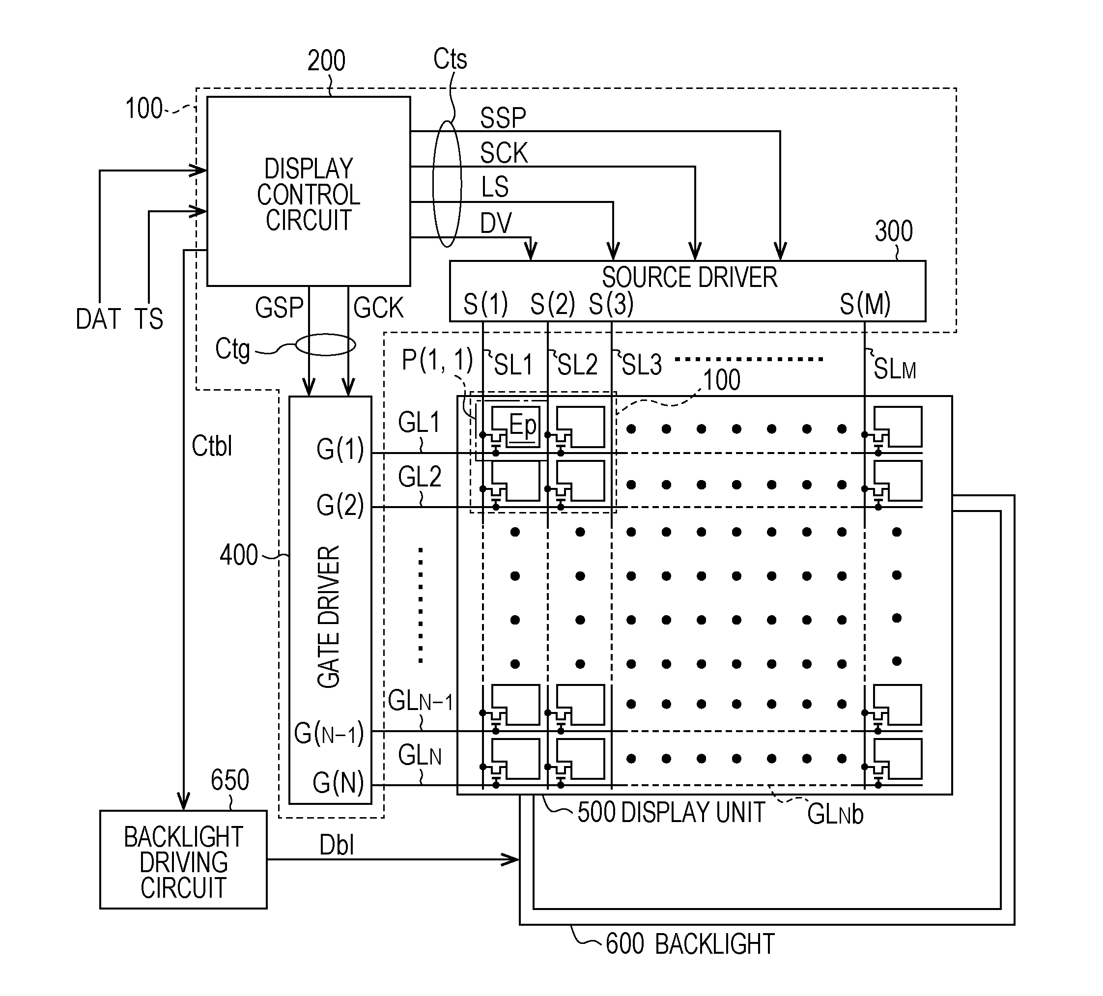
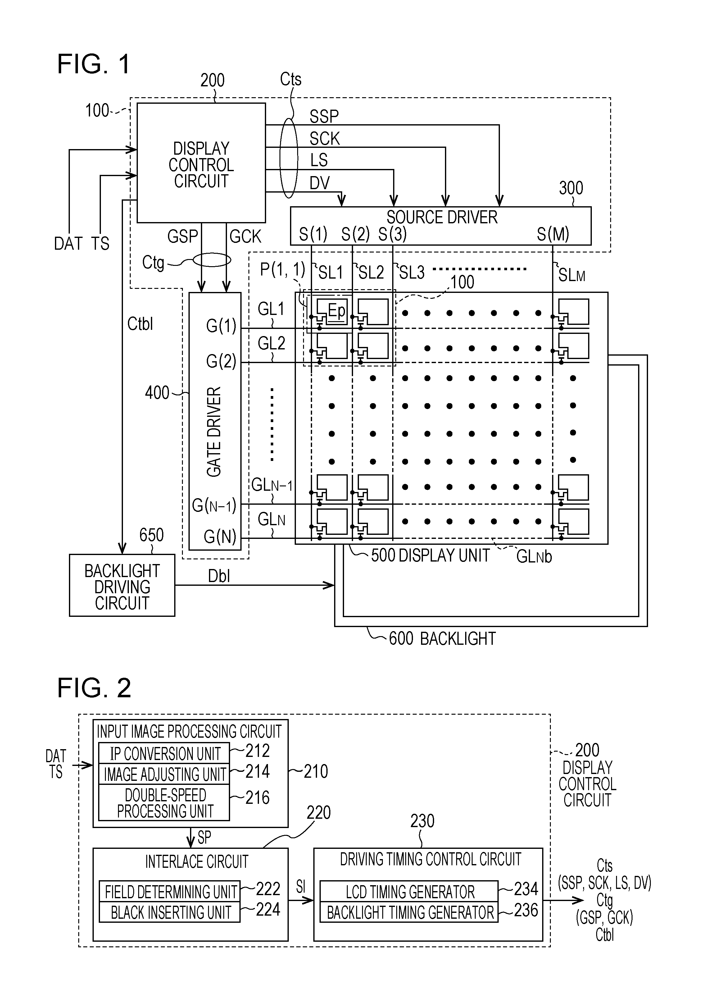
[0074]FIG. 1 is a block diagram illustrating a configuration of an active-matrix-type liquid crystal device according to a first embodiment of the present invention. This liquid crystal device includes a display unit 500 which is a liquid crystal panel conforming to the normally black mode, a display driving circuit 100 configured to drive the display unit 500 thereof, a backlight 600 serving as a planar lighting device configured to irradiate light on the rear face of the display unit 500 (liquid crystal panel), and a backlight driving circuit 650 configured to drive the backlight 600 thereof. The display driving circuit 100 includes a source driver 300 serving as a data signal line driving circuit, a gate driver 400 serving as a scanning signal line driving circuit, and a display control circuit 200, and this display control circuit 200 controls the source driver 300, gate driver 400, and backlight driving circuit 650. An image signal DAT ...

second embodiment

2. Second Embodiment

[0105]Next, a liquid crystal display device according to a second embodiment of the present invention will be described. The entire configuration of the liquid crystal device according to the present embodiment is as illustrated in FIG. 8, and basically the same as the entire configuration of the first embodiment (FIG. 1), but the configuration of the display unit 500 differs from that in the first embodiment. Therefore, hereinafter, description will be made with this different point as the center, and with configurations other than this different point, the same or corresponding portions are denoted with the same reference numerals, and detailed description will be omitted.

[0106]FIG. 10 is a partially enlarged view schematically illustrating electric connection configuration within the display unit 500 in the present embodiment illustrated in FIG. 8, “+” or “−” appended to each pixel electrode in FIG. 10 indicates the polarity of voltage (pixel voltage) to be ap...

third embodiment

3. Third Embodiment

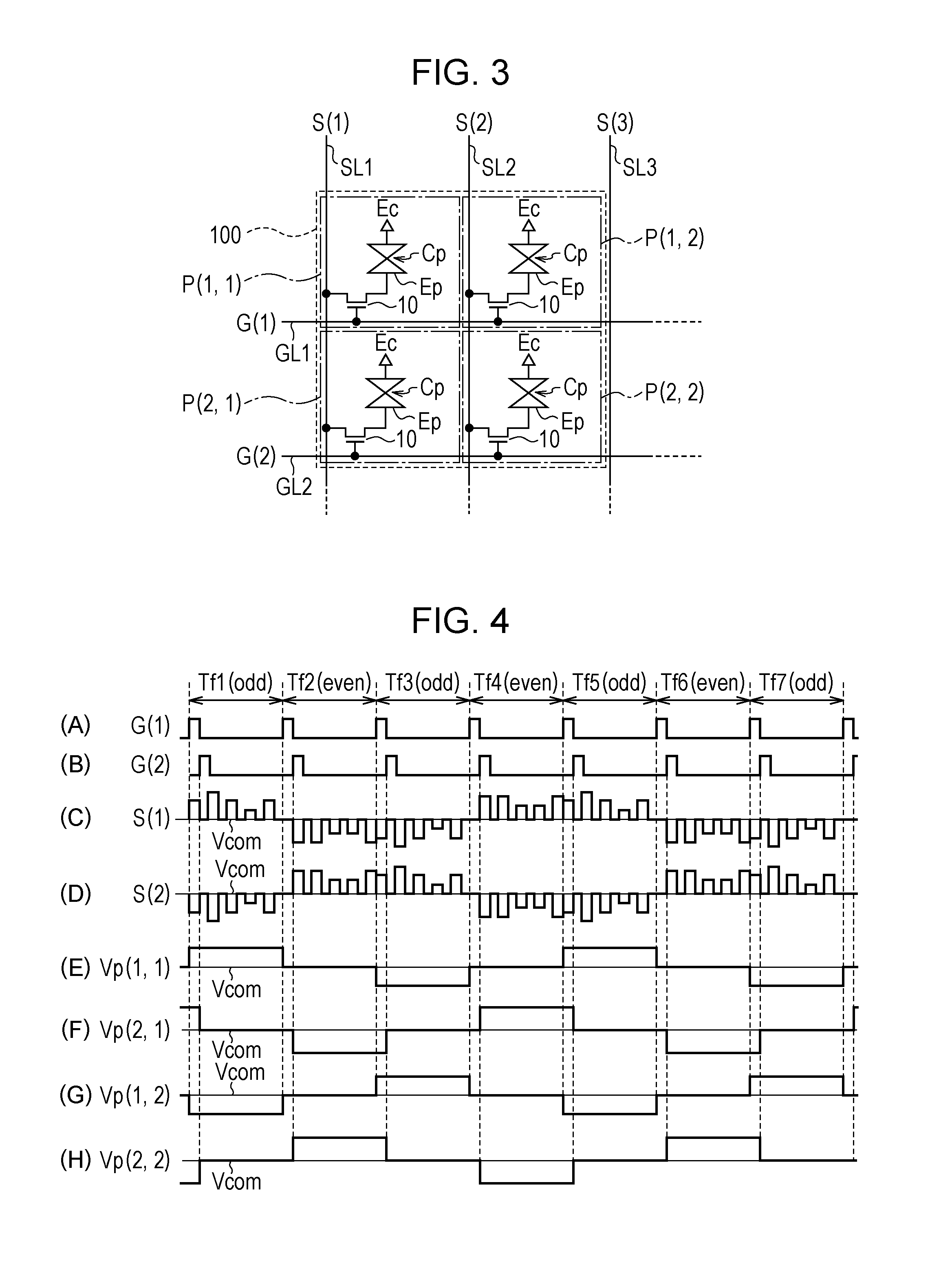
[0129]With the first and second embodiments, when focusing on the pixel formation units P(i, j), double-speed interlace display is performed wherein a frame which forms a pixel of an image to be displayed (hereinafter, referred to as “display frame”) and a frame which forms a black pixel (hereinafter, referred to as “black frame”) alternately appear ((E) to (H) in FIG. 4, (E) to (H) in FIG. 13), and accordingly, the state of the liquid crystal at the time of starting of each display frame is stable, and it is thought that there is no particularly need to drive the liquid crystal with driving voltage in which temporal change in a gradation value is enhanced to compensate for optical responsiveness of the liquid crystal (called “overshoot drive” or “OS drive”). However, as a result of the inventor of the present application performing study regarding this point, it was found that the final arrival state (transmittance) of the liquid crystal in a black frame depends ...


PUM


Abstract

A display control circuit of a liquid crystal display device generates a double-speed progressive image signal by changing an input image signal based on interlaced scanning into a progressive scanning mode, and also by doubling the frame frequency. With the double-speed progressive image signal, a pixel value equivalent to an odd-numbered scanning line in an odd-numbered frame remains unchanged, a pixel value equivalent to an even-numbered scanning line is replaced with a black pixel value, a pixel value equivalent to an even-numbered scanning line in an even-numbered frame remains unchanged, and a pixel value equivalent to an odd-numbered scanning line is replaced with a black pixel value. An image that the double-speed interlace image signal represents is displayed on a liquid crystal panel.

Description

TECHNICAL FIELD[0001]The present invention relates to an active-matrix-type display device such as a liquid crystal display device using a switching element such as a thin-film transistor or the like, and a driving method thereof.BACKGROUND ART[0002]In order to display an image on a display panel such as a liquid crystal panel having large capacitance or the like using image signals conforming to the interlaced format such as television signals, there has known a format such as a system for driving two lines of a display panel at the same time using one-line signal during each field period (called “line doubler system”). According to use of this line doubler system, an image can be displayed on a large-capacitance display panel using signals conforming to the interlaced format, but the image that an image signal thereof represents cannot be displayed in a suitable manner. Specifically, of image signals conforming to this interlaced format, in the event that signals equivalent to two...

Claims


Application Information

Patent Timeline
Patent Type & Authority Patents(United States)
IPC IPC(8): G09G3/36G09G3/34
CPCG09G3/36G09G3/3648G09G3/342G09G3/3614G09G3/3655G09G2300/0426G09G2310/024G09G2310/0224G09G2310/061G09G2310/08G09G2320/0247G09G2320/0252G09G2320/0261G09G2340/16
Inventor SHIOMI, MAKOTO
Owner SHARP KK
Why Eureka
Try Eureka