Organic light emitting display device including a non-light emitting region, light emitting region and photochromic layer

a light emitting display and organic technology, applied in the field of display devices, can solve the problems of deterioration of the light emitting efficiency of the organic light emitting display devices, and achieve the effect of preventing the deterioration of visibility

Active Publication Date: 2016-11-01
SAMSUNG DISPLAY CO LTD
View PDF28 Cites 4 Cited by
  • Summary
  • Abstract
  • Description
  • Claims
  • Application Information

AI Technical Summary

Benefits of technology

[0007]In order to prevent the visibility deterioration due to the reflection of an external light, a circular polarizer or a photochromic (Ph) layer may be arranged on an upper portion of the organic light emitting display device as an external light reflection prevention member. However, due to the arrangement of the external light reflection prevention member, light that is emitted from the organic light emitting display device may be absorbed by or in the external light reflection prevention member, and thus the light emitting efficiency of the organic light emitting display device may deteriorate.
[0008]Accordingly, an aspect of the present invention provides an organic light emitting display device which can prevent deterioration of the light emitting efficiency while reducing (e.g., minimizing) the external light reflection of a screen.
[0009]Another aspect of the present invention provides an organic light emitting display device which can improve the display quality by or through prevention of deterioration of the light emitting efficiency while lowering (e.g., minimizing) the external light reflection of a screen.

Problems solved by technology

However, due to the arrangement of the external light reflection prevention member, light that is emitted from the organic light emitting display device may be absorbed by or in the external light reflection prevention member, and thus the light emitting efficiency of the organic light emitting display device may deteriorate.

Method used


Image

  • Organic light emitting display device including a non-light emitting region, light emitting region and photochromic layer
  • Organic light emitting display device including a non-light emitting region, light emitting region and photochromic layer
  • Organic light emitting display device including a non-light emitting region, light emitting region and photochromic layer

Examples


Embodiment Construction

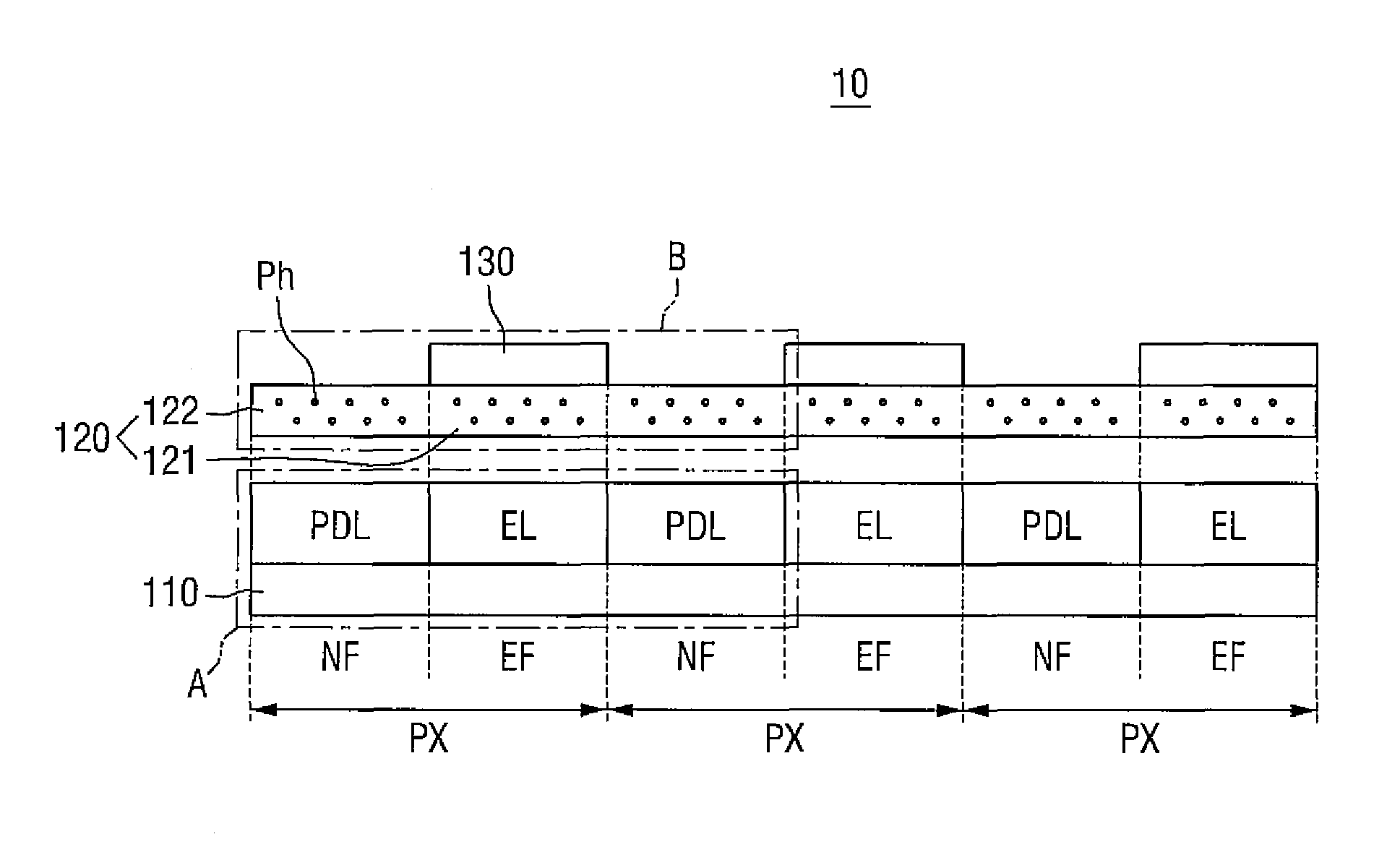
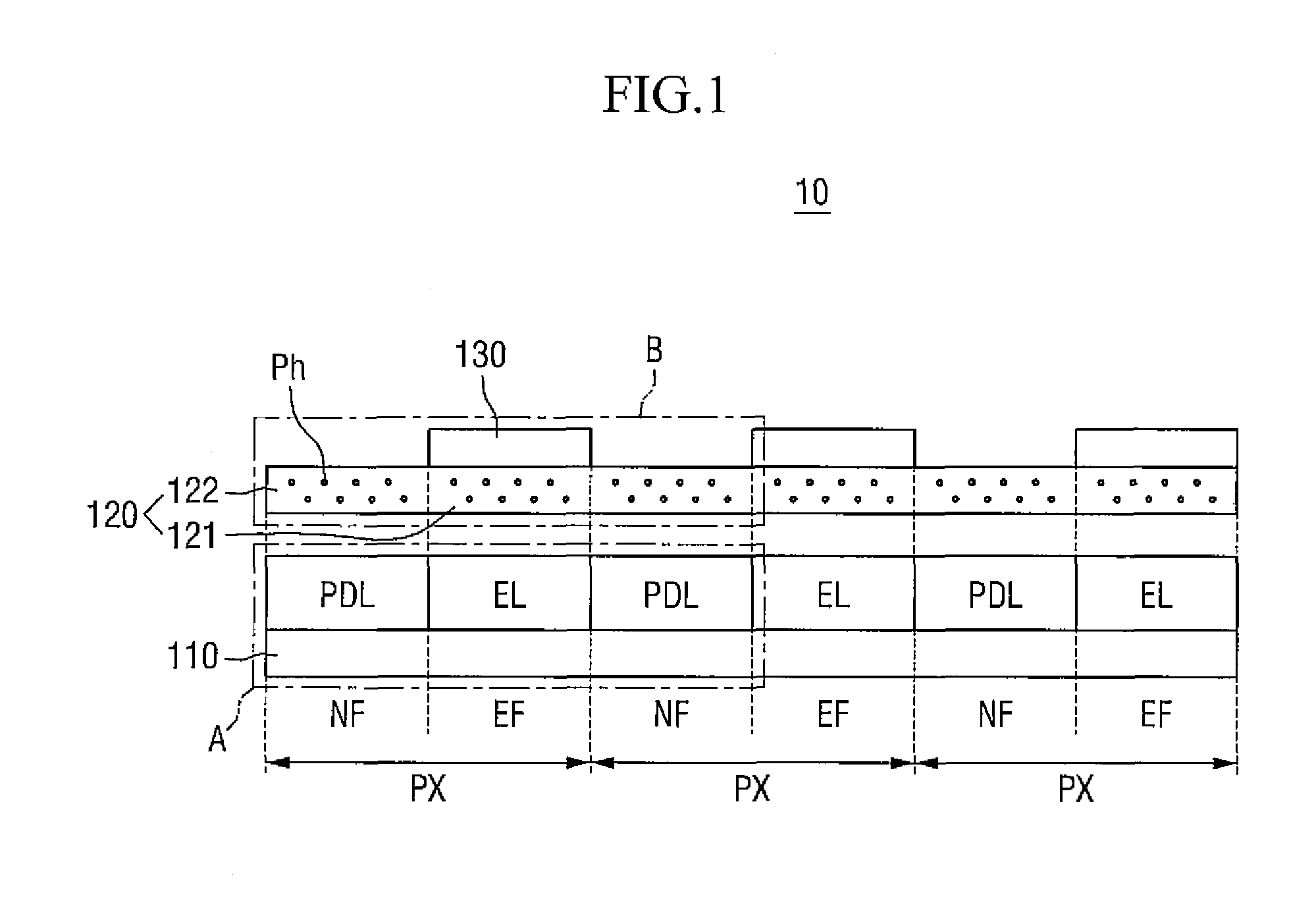
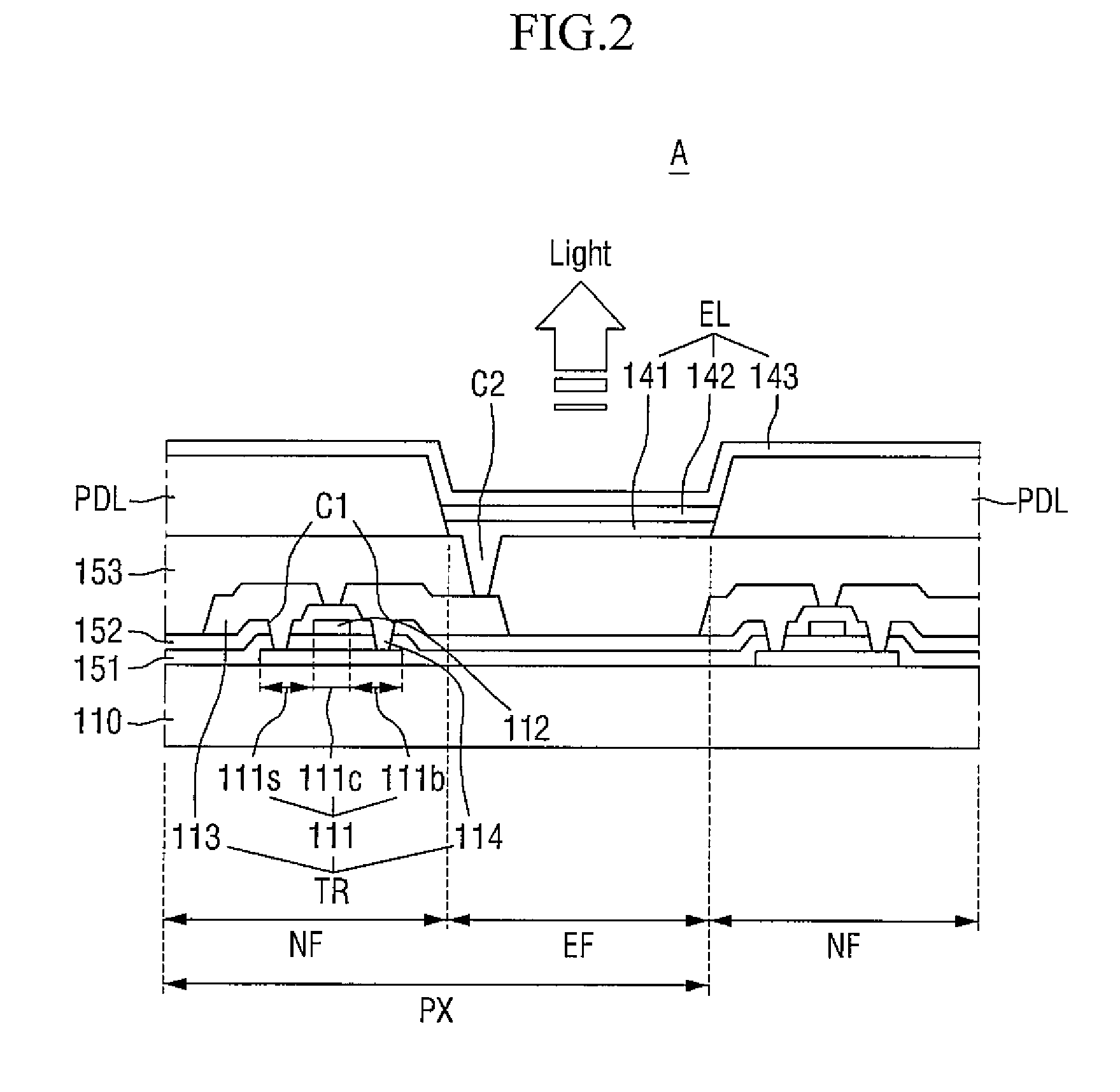
[0048]Aspects and features of the present invention and methods of accomplishing the same may be understood more readily by reference to the following detailed description of example embodiments and the accompanying drawings. The present invention may, however, be embodied in many different forms and should not be construed as being limited to the embodiments set forth herein. Rather, these embodiments are provided so that this disclosure will be thorough and complete and will fully convey the concept of the invention to those skilled in the art, and the present invention will be defined by the appended claims and their equivalents. Thus, in some embodiments, well-known structures and devices may not be shown in order not to obscure the description of the invention with unnecessary detail. Like numbers refer to like elements throughout. In the drawings, the thickness of layers and regions are exaggerated for clarity.

[0049]It will be understood that when an element or layer is referr...


PUM


Abstract

An organic light emitting display device includes a substrate having a non-light emitting region and a light emitting region, a photochromic layer in a path of light that is emitted from the light emitting region and a light blocking layer on the photochromic layer, wherein the light blocking layer comprises a plurality of light blocking patterns that are spaced from each other, the light blocking patterns overlap the light emitting region, and a space between adjacent light blocking patterns exposes the non-light emitting region.

Description

CROSS-REFERENCE TO RELATED APPLICATION[0001]This application claims priority to and the benefit of Korean Patent Application No. 10-2013-0096698 filed on Aug. 14, 2013 in the Korean Intellectual Property Office, the disclosure of which is incorporated herein in its entirety by reference.BACKGROUND[0002]1. Field[0003]The present invention relates to a display device, and more particularly to an organic light emitting display device.[0004]2. Description of the Related Art[0005]Unlike a liquid crystal display (LCD), an organic light emitting display device is self-luminescent without the necessity of a separate light source, and thus its thickness and weight can be reduced. Further, the organic light emitting display device has the advantages of wide viewing angle, low power consumption, high luminance, and high response speed, and has been actively developed as the next-generation display device.[0006]The organic light emitting display device includes thin-film transistors and organic...

Claims


Application Information

Patent Timeline
Patent Type & Authority Patents(United States)
IPC IPC(8): H01L29/08H01L35/24H01L51/00H01L51/52H01L27/32
CPCH01L51/5284H01L27/3244H10K59/122H10K50/865H10K50/84H10K59/12
Inventor CHOI, CHUNG SOCKKANG, JIN KOOKIM, SOO YOUNKIM, SEUNG HUNKIM, HYUN HOSONG, SEUNG YONGJANG, CHEOLCHO, SANG HWANPARK, SANG HYUN
Owner SAMSUNG DISPLAY CO LTD
Why Eureka
Try Eureka