Conductive film and display device including the same

a display device and conductive film technology, applied in the direction of conductive layers on insulating supports, instruments, computing, etc., can solve the problems of increasing the capacity of electronic data, difficult to improve the visibility of single patterns, and difficult to handle data, so as to reduce the generation of noise, improve visibility and a display device, and improve image quality.

Active Publication Date: 2019-07-23
FUJIFILM CORP
View PDF17 Cites 2 Cited by
  • Summary
  • Abstract
  • Description
  • Claims
  • Application Information

AI Technical Summary

Benefits of technology

[0007]In JP2014-519129A, in order to improve the visibility of the transparent electrode region, it is suggested that a metal electrode is formed with a random irregular mesh so as to have a random mesh pattern.
[0011]Therefore, in order to prevent visibility deterioration due to repetition of the small piece of the random mesh pattern, it is required to provide constraints during the forming of electronic data of the random mesh pattern. That is, it is important to define a combination of a display and a random pattern for improving visibility.
[0012]An object of the present invention is to provide a conductive film having a random (irregular) mesh-like wiring pattern (mesh pattern) capable of suppressing generation of a noise recognized in combination with a display unit (display) and improving visibility and a display device including the same.
[0013]Particularly, an object of the present invention is to provide a conductive film having a random mesh pattern that may have combination with a mesh pattern and a display that can provide the best image quality in which the moire and also the noise are not recognized or hardly recognized in the design of a random mesh pattern in a case where the openings of the red (R), green (G), and blue (B) subpixels of the display have different frequencies and intensities and a display device including the same.
[0018]As described above, according to the present invention, it is possible to provide a conductive film having a random (irregular) mesh-like wiring pattern (mesh pattern) capable of suppressing generation of a noise recognized in combination with a display unit (display) and improving visibility and a display device including the same.
[0019]Particularly, it is possible to provide a conductive film having a random mesh pattern that may have combination with a mesh pattern and a display that can provide the best image quality in which the moire and also the noise are not visually recognized or hardly visually recognized in the design of a random mesh pattern in a case where the openings of the red (R), green (G), and blue (B) subpixels of the display have different frequencies and intensities and a display device including the same.

Problems solved by technology

However, by the overlapping with the display, the random mesh pattern generates a variety of noises, and thus there is a problem in that it is difficult to improve the visibility thereof in a single pattern.
In a case where a random mesh pattern is provided as vector data, as the size of the display to be applied increases, the capacity of the electronic data increases, and thus handling of the data becomes difficult in some cases.
However, in this case, it is known that there is a problem in that visibility is deteriorated due to the repetitive structure.
For example, in a case where a display is formed with a small piece of the random pattern, unless a certain constraint condition is not provided, there is a problem in that the repeating shape as illustrated in FIG. 25 is conspicuous and is easily recognized.

Method used


Image

  • Conductive film and display device including the same
  • Conductive film and display device including the same
  • Conductive film and display device including the same

Examples


first embodiment

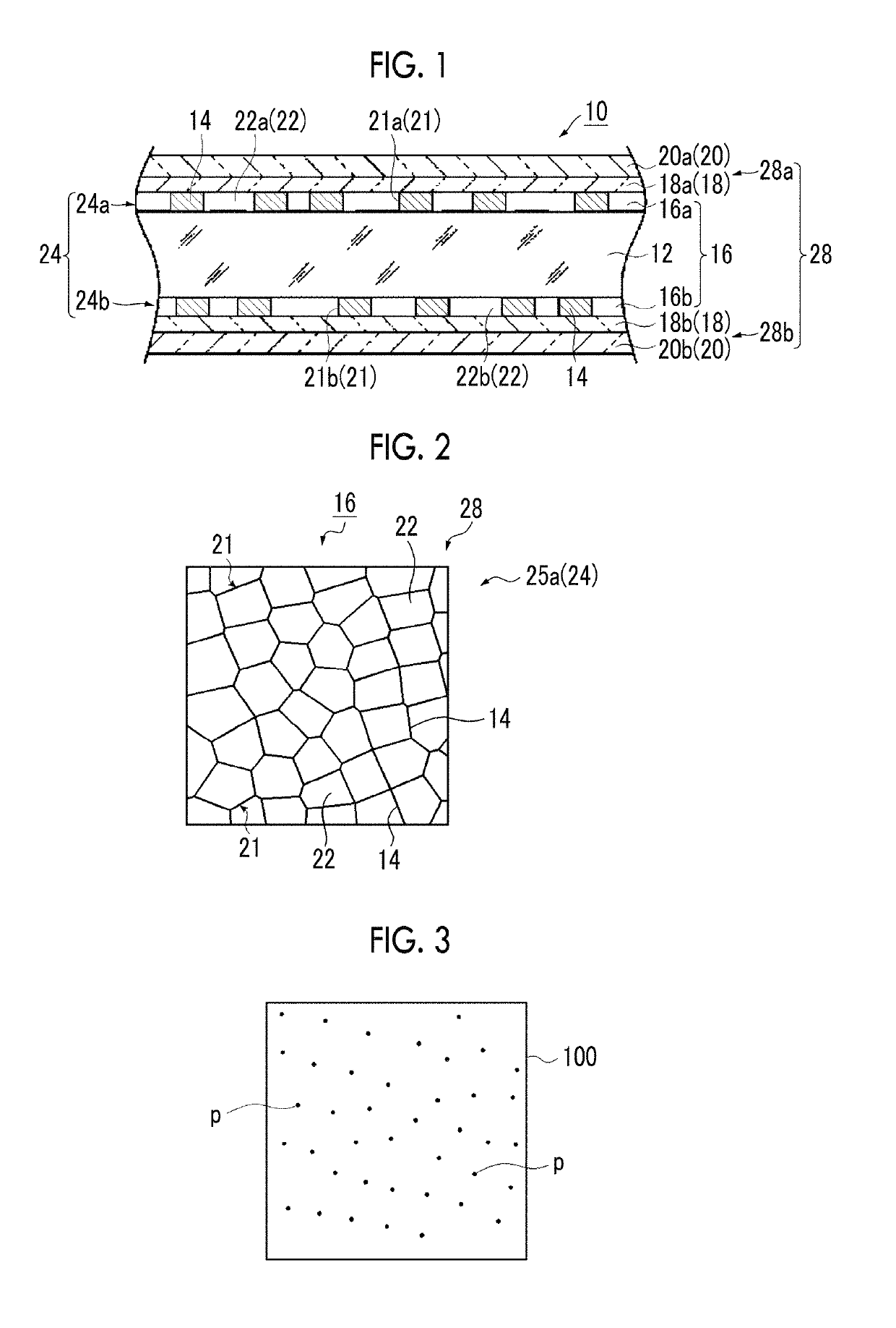
[0084]FIG. 1 is a partial cross-sectional view schematically illustrating an example of a conductive film according to the present invention, and FIG. 2 is a plan view schematically illustrating an example of a wiring pattern of a wiring portion of the conductive film illustrated in FIG. 1.

[0085]As illustrated in these drawings, a conductive film 10 according to the present embodiment is a conductive film that is provided on a display unit of a display device and that has a wiring pattern excellent in view of restraining the generation of a noise with respect to a black matrix (BM) of the display unit, particularly, a wiring pattern optimized in view of visibility of a noise with respect to a BM pattern in a case where of being overlapped with a BM pattern and has a transparent base body 12; a first wiring portions 16a that is formed on one surface (upper surface in FIG. 1) of the transparent base body 12, that is formed of a plurality of metal thin wires (hereinafter, referred to a...

second embodiment

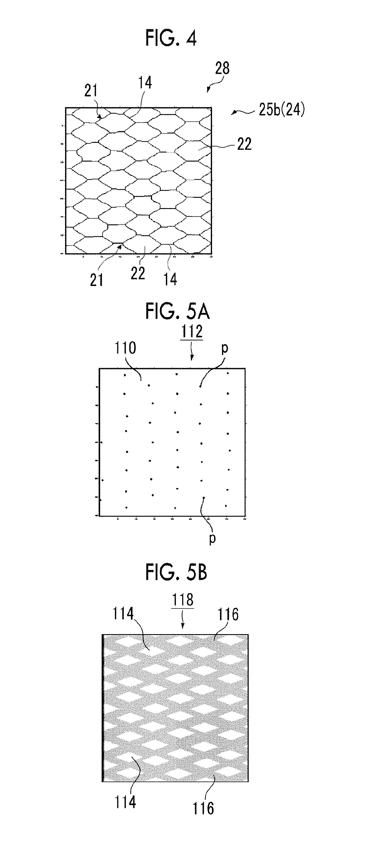
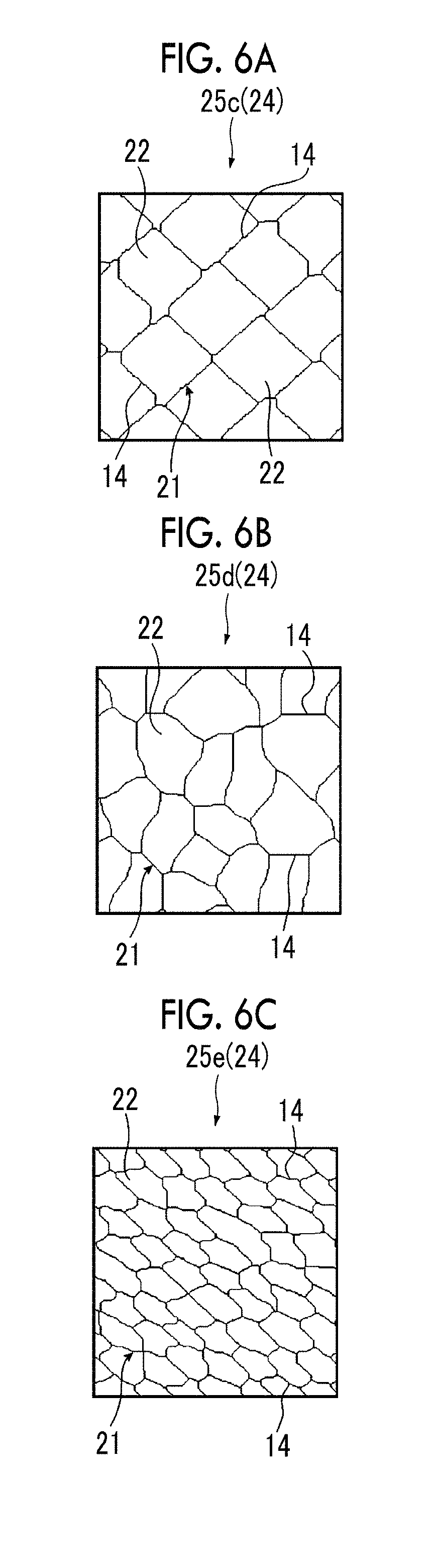
[0116]Otherwise, as illustrated in FIG. 9, as described above, at least one of the plurality of metal thin wires 14 of the first and second wiring portions 16a and 16b is divided by the disconnection (break) to an electrode portion 17 forming the wiring layer 28 and dummy electrode portions (non-electrode portions) 26, any one of the electrode portion 17 and the dummy electrode portions 26 is formed with the plurality of metal thin wires 14 having the random mesh pattern 25a as illustrated in FIG. 2, and the other thereof is formed with the plurality of metal thin wires 14 having the regular fixed pattern 27 (with reference to FIG. 8), so as to obtain a form such as a conductive film 11 of the present invention as illustrated in FIG. 10 described below. In this manner, irregularity may be applied to the composite wiring pattern obtained by the combination of the random mesh pattern 25a and the regular fixed pattern 27 and the overlapping with the random mesh pattern 25a or the fixed...

third embodiment

[0143]In FIG. 11, the conductive film 11A of the present invention illustrated in FIG. 11 has the lower transparent base body 12b, the second wiring portion 16b formed of the plurality of metal thin wires 14 formed on the upper surface of the transparent base body 12b, the second protective layer 20b adhered to the second wiring portion 16b via the second adhesive layer 18b, the upper transparent base body 12a arranged to be adhered to the second protective layer 20b, for example, by an adhesive or the like, the first wiring portion 16a formed of the plurality of metal thin wires 14 formed on the upper surface of the transparent base body 12a, and the protective layer 20a that is adhered to the first wiring portion 16a via the adhesive layer 18a.

[0144]Here, all or a portion of at least one of the first wiring portion 16a and the metal thin wire 14 of the second wiring portion 16b is the random mesh pattern 25a to which the irregularity is applied illustrated in FIG. 2.

[0145]In the ...


PUM

PropertyMeasurementUnit
lengthaaaaaaaaaa
lengthaaaaaaaaaa
lengthaaaaaaaaaa

Abstract

With respect to a conductive film according to the present invention, in a case where in one or more metal thin wires forming a irregular wiring pattern, one continuous line segment which extends in the longitudinal direction of the subpixels of the display unit and which can be regarded as one traverse one or more subpixels in the longitudinal direction, in a case where a total length of one or more traverse subpixels in which the one line segment is traversed in the longitudinal direction is set as a length L μm and a coverage in which one line segment covers one or more traverse subpixels is set as C %, the length L and the coverage C of one line segment of the irregular wiring pattern that is overlapped with a pixel arrangement pattern of the display unit are included in a region below a line represented by equations below,in a case where 0<x≤168, y=6.7,in a case where 168<x≤252, y=−0.00595x+7.7,in a case where 252<x≤378, y=−0.00476x+7.4,in a case where 378<x≤504, y=−0.02143x+13.7, andin a case where 504<x≤756, y=2.9.

Description

CROSS-REFERENCE TO RELATED APPLICATIONS[0001]This application is a Continuation of PCT International Application No. PCT / JP2016 / 079793 filed on Oct. 6, 2016, which claims priority under 35 U.S.C. § 119(a) to Japanese Patent Application No. 2015-204748 filed on Oct. 16, 2015. The above application is hereby expressly incorporated by reference, in its entirety, into the present application.BACKGROUND OF THE INVENTION1. Field of the Invention[0002]The present invention relates to a conductive film and a display device including the same, and specifically, a conductive film in which a noise due to the interference with a display device is suppressed and a mesh-like wiring pattern having excellent visibility is provided, and a display device.2. Description of the Related Art[0003]Examples of a conductive film provided on a display unit of a display device (hereinafter, referred to as a display) include a conductive film for a touch panel having a conductive film formed of a metal thin wi...

Claims


Application Information

Patent Timeline
Patent Type & Authority Patents(United States)
IPC IPC(8): G06F3/044H05K9/00G02F1/1333
CPCG06F3/044G02F1/13338H05K9/0096G06F2203/04112G06F2203/04103G06F3/0445G06F3/0446G06F3/041H01B5/14
Inventor IWAMI, KAZUCHIKA
Owner FUJIFILM CORP
Why Eureka
Try Eureka