Packaging structure for a laser diode

a laser diode and packaging technology, applied in the direction of lasers, semiconductor laser arrangements, semiconductor lasers, etc., can solve the problems of difficult to expand the heat-conducting area, difficult to implement the packaging structure for high-power laser diodes, and difficult to dissipate the amount of heat generated by the laser diode chip

Active Publication Date: 2016-11-15
LEE HOU CHIEH
View PDF3 Cites 1 Cited by
  • Summary
  • Abstract
  • Description
  • Claims
  • Application Information

AI Technical Summary

Benefits of technology

[0010]One goal of the present invention is to provide a packaging structure for a laser diode chip, especially one used for a medium or high power laser diode, the packaging structure has a larger faying plane between an electrically insulated, heat-conducting board and a heat-conducting base, and the area size of the faying plane can be adjusted according to the power of the laser diodes, their shapes can be rectangular, square or irregular, which can efficiently and rapidly conduct and dissipate the heat generated by the laser diodes to extend the service life of the laser diodes. Besides, the output optical power of the laser diodes can be increased at the same driving current since the heat dissipation has been improved.
[0011]Another goal of the present invention is to provide a packaging structure for a laser diode, wherein the optical axis of the laser diodes is generally parallel to the surface of the electrically insulated, heat-conducting board, and the assembling process is simpler and the cost for assembling is decreased.
[0012]Another goal of the present invention is to provide a packaging structure for a laser diode, in which there is a space for additional devices, such as a photo diode to measure the optical power of the laser diode, a reverse bias voltage protection diode, and / or an electrostatic discharge protection diode to improve the performance and to extend the service life of the laser diode.
[0013]Another goal of the present invention is to provide a packaging structure for a laser diode, wherein the electrically insulated, heat-conducting board and the heat-conducting base are coincided into a single electrically insulated, heat-conducting component, which can conduct and dissipate the heat rapidly and efficiently and reduce the packaging cost.

Problems solved by technology

However, the aforementioned packaging structure is difficult to be implemented for high-power laser diodes, because high-power laser diodes generate a much larger amount of heat.
According to physics, one skilled in the art should know that the rate of heat conduction is proportional to the heat-conducting area, and because the heat-conducting area of the submount provided by the conventional packaging structure for a laser diode (the aforementioned area of the faying plane) is too small, the large amount of heat generated by the laser diode chip is difficult to be dissipated through the submount to the heat-conducting base; furthermore, because the submount is installed in a limited space, the heat-conducting area cannot be expanded as necessary for improving the heat-conducting efficiency.
Furthermore, as shown in FIG. 1 and FIG. 2, the conventional laser diodes are packaged cylindrically and individually, as previously discussed the heat-conducting area of the submount cannot be expanded inside the package, and there is no space to accommodate another laser diode chip, nor other electronic components.
Apparently, the conventional packaging is not suitable for a device that needs more than one laser diode, and there is no space for installing other electronic components to improve performance.
Besides, the existing packaging methods for laser diodes cannot provide additional space in the existing packaging structure to improve the performance of the laser diode, for example, an additional photo diode for detecting the optical power of laser diodes, an electrostatic discharge protection diode, and / or a reverse bias voltage protection diode.
Besides, one skilled in the art also knows the LED chip emits light from the upfront surface instead of edge, it is easy for the LED to be packaged on a large plate for large amount heat dissipation; however, most of the laser diode chips emit light from the edge instead of the upfront surface, it is difficult for them to be packaged on a large plate.
Consequently, conventional laser diode chips that emit light from the edge are not packaged on a large plate and cannot be provided with large size heat-conducting components.

Method used


Image

  • Packaging structure for a laser diode
  • Packaging structure for a laser diode
  • Packaging structure for a laser diode

Examples


Embodiment Construction

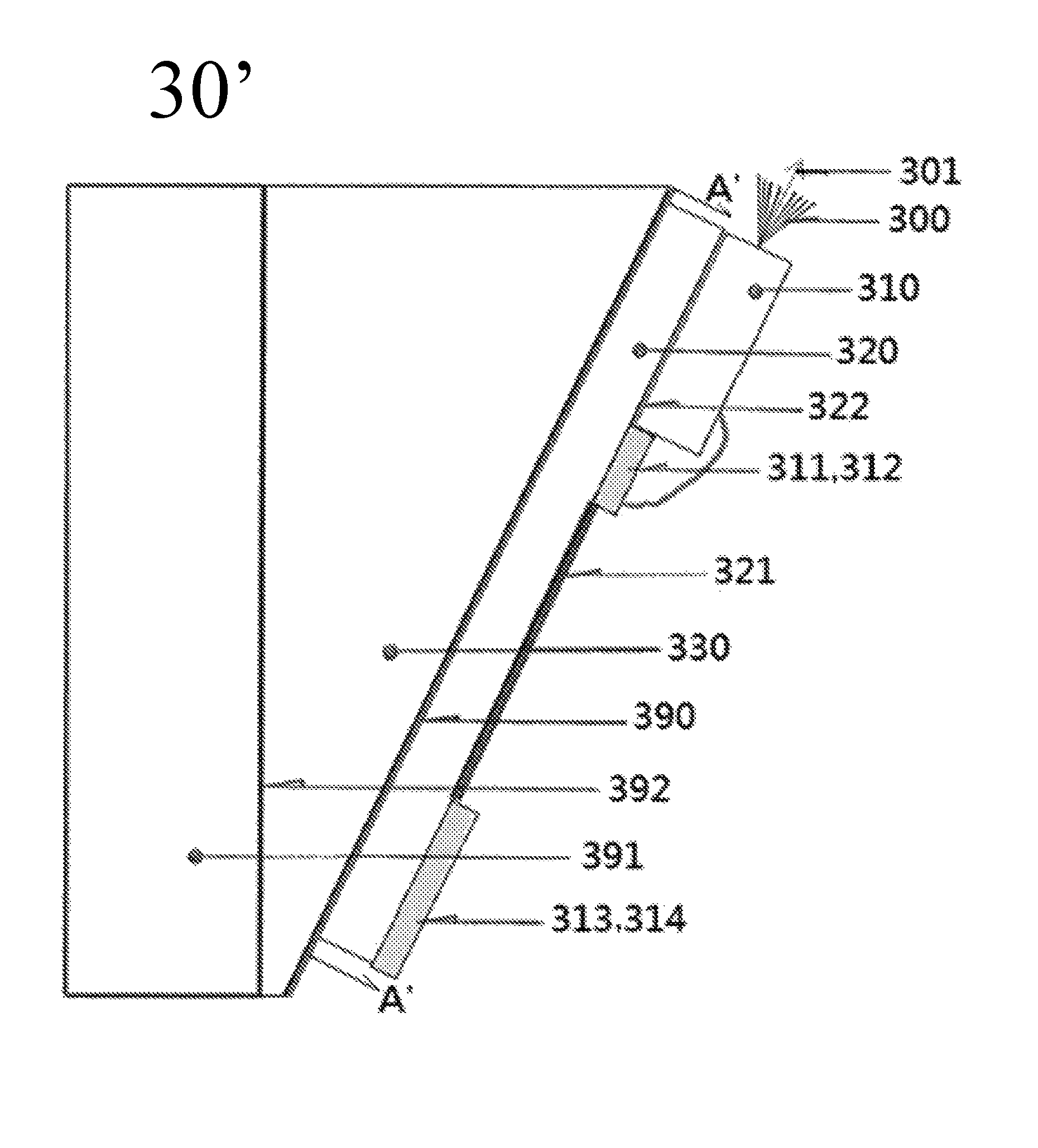
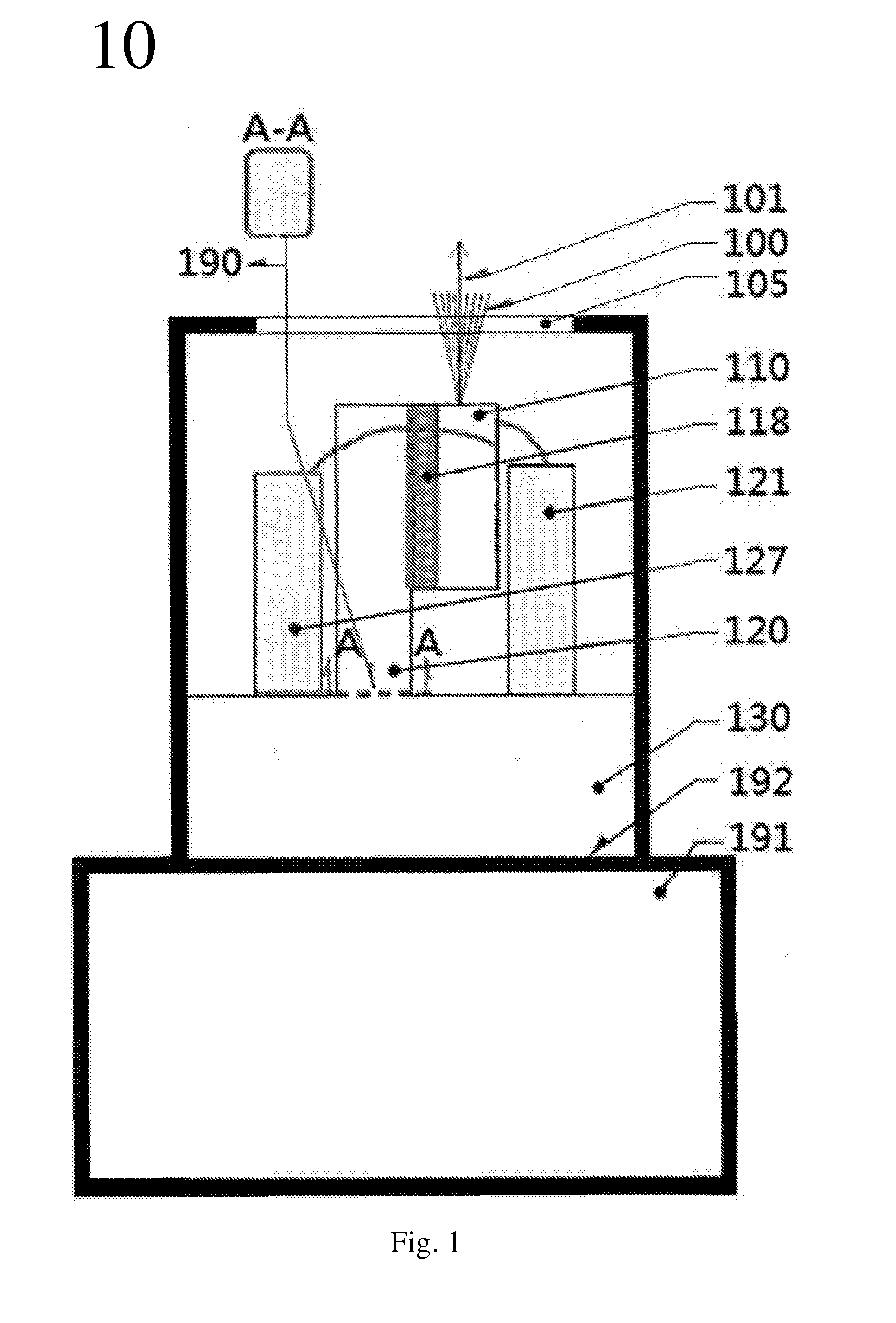
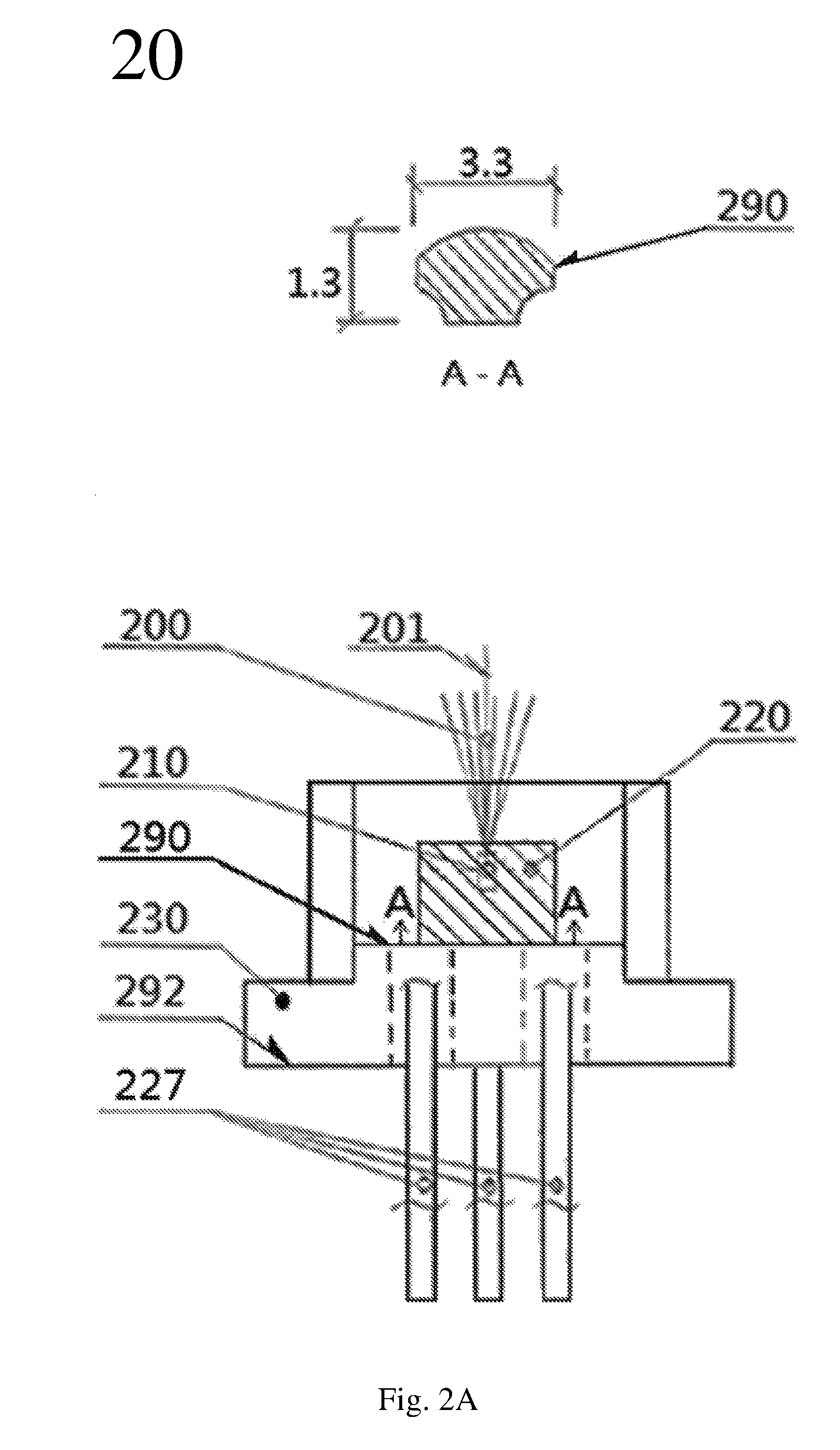
[0009]The present invention provides an electrically insulated, heat-conducting board, when used as a component for packaging, it is similar to a submount (a component used for fixing and installing laser diode chips) of a conventional packaging structure for a laser diode, but totally different from a submount in its configuration, shape and size of the area.

[0010]One goal of the present invention is to provide a packaging structure for a laser diode chip, especially one used for a medium or high power laser diode, the packaging structure has a larger faying plane between an electrically insulated, heat-conducting board and a heat-conducting base, and the area size of the faying plane can be adjusted according to the power of the laser diodes, their shapes can be rectangular, square or irregular, which can efficiently and rapidly conduct and dissipate the heat generated by the laser diodes to extend the service life of the laser diodes. Besides, the output optical power of the lase...


PUM


Abstract

The invention relates to a packaging structure for a laser diode, comprising an electrically insulated, heat-conducting board having an electronic circuit thereon; a laser diode chip mounted on the electronic circuit of the electrically insulated, heat-conducting board and having an anode and a cathode, respectively connected to an external soldering pad for external electrical connections; and a heat-conducting base installed on a surface of the electrically insulated, heat-conducting board to conduct the heat generated by the laser diode chip to the heat-conducting base through the electrically insulated, heat-conducting board, wherein the laser diode chip emits the light from an edge of the electrically insulated, heat-conducting board and the area of a faying plane between the electrically insulated, heat-conducting board and the heat-conducting base is adjusted depending on the power requirements of the laser diode, and the area of the faying plane is from 6 to 5,000 mm2.

Description

CROSS-REFERENCES TO RELATED APPLICATIONS[0001]The present application claims priority to Taiwan Patent Application No. 104204856 filed on Mar. 31, 2015, incorporated herein by reference in its entirety.FIELD OF THE INVENTION[0002]The present invention relates to a packaging structure for a laser diode, specifically, relating to a packaging structure which is a heat-conducting component capable of creating a larger heat-conducting area of a faying plane between a submount for the laser diode chip and a heat-conducting base, so that the heat generated by the laser diode can be rapidly and effectively conducted and dissipated.BACKGROUND OF THE INVENTION[0003]As shown in FIG. 1, a conventional packaging structure for a laser diode 10, comprises: a laser diode chip 110, an optical axis 101 of a light beam center capable of emitting a cone-shaped laser beam 100, a submount 120, and a heat-conducting base 130, wherein the submount 120 and the heat-conducting base 130 are made of copper all...

Claims


Application Information

Patent Timeline
Patent Type & Authority Patents(United States)
IPC IPC(8): H01S5/024H01S5/068H01S5/022H01S5/40
CPCH01S5/02469H01S5/02248H01S5/02252H01S5/02272H01S5/06825H01S5/4025H01S5/02212H01S5/02476H01L2224/48091H01S5/0237H01S5/02325H01L2924/00014H01S5/02355H01S5/02326
Inventor LEE, HOU-CHIEHLEE, HSUN-FU
Owner LEE HOU CHIEH
Why Eureka
Try Eureka