

Nanoscale metal oxide resistive switching element
a metal oxide resistive switching and metal oxide technology, applied in the field of nonvolatile switching and memory devices, can solve the problems of incompatibility with cmos processing, limited device size, and limited further device size shrinkage, etc., to achieve low current for programming, reduce power consumption in operation, and flexible thermal budget for device fabrication
- Summary
- Abstract
- Description
- Claims
- Application Information
AI Technical Summary
Benefits of technology
Problems solved by technology
Method used
Image

Examples
Embodiment Construction
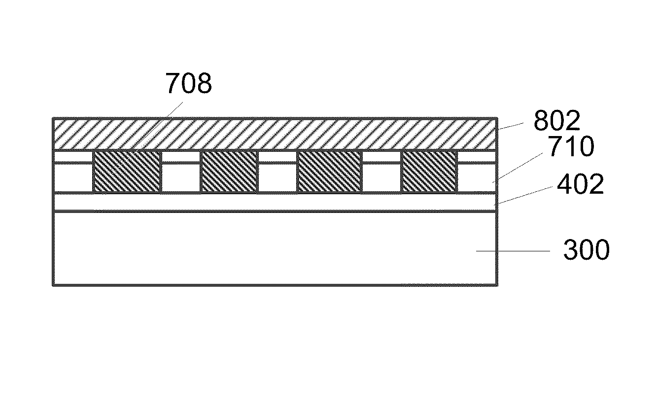
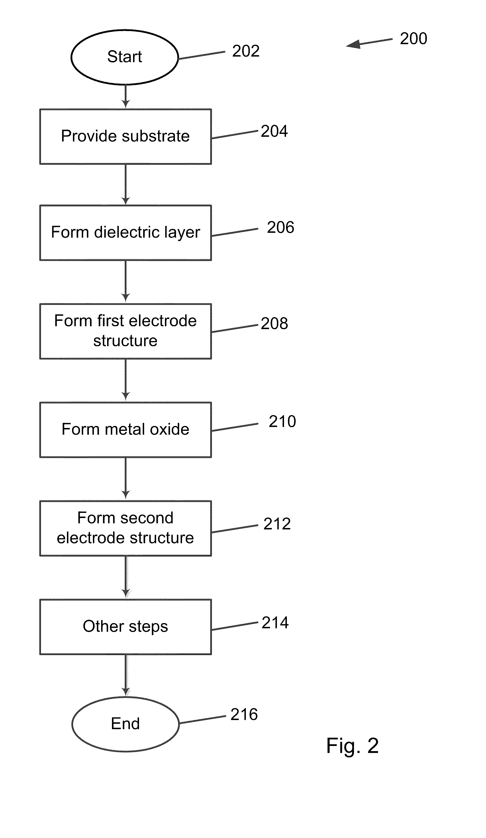
[0018]Resistive switching for memory devices usually includes a change of an electric resistance of a switching element sandwiched between two electrodes. The change of the electric resistance of the switching device can be brought about by an injection or redistribution of conductive entities into the switching element when a voltage or a current is applied to the electrodes. Depending on the device structure, the resistance of the switching element may be changed by using mechanisms such as conductor particles formation, electrochemical reactions or cation / anion migration or even oxygen migration in the switching medium, and others, depending on the application.
[0019]Accordingly, the illustrated embodiments are related to switching devices. More particularly, the illustrated embodiments provide a structure and a method for forming a resistive switching device using a metal oxide as a switching material. The switching device has been used in a non-volatile memory device, but other ...
PUM
| Property | Measurement | Unit |
|---|---|---|
| width | aaaaa | aaaaa |
| width | aaaaa | aaaaa |
| thickness | aaaaa | aaaaa |
Abstract
Description
Claims
Application Information