Flexible display device with side crack protection structure and manufacturing method for the same

a flexible display and side crack protection technology, applied in the field of electronic devices with a display, can solve the problems of unappealing device aesthetics, difficult to incorporate the display panel into the housing of electronic devices, and bulky display panels

Active Publication Date: 2017-01-10
LG DISPLAY CO LTD
View PDF16 Cites 15 Cited by
  • Summary
  • Abstract
  • Description
  • Claims
  • Application Information

AI Technical Summary

Benefits of technology

[0012]An aspect of the present disclosure is related to a flexible display, which includes configurations for wire traces to withstand bending stress for reliable operation of the flexible display.
[0013]In one embodiment, a flexible display includes an active area provided with a plurality of pixels and one or more inactive areas at the periphery of the active area. The inactive area positioned at one or more side of the active area includes a bend allowance section with a plurality of conductive line traces. The inactive area with the bend allowance section is notched. Between the notched line and the closest conductive line trace of the bend allowance section, the buffer layer on the base layer is etched so that a buffer layer etched area is provided therein. With the buffer layer removed from the area between the notched line and the conductive line trace, cracks initiation and propagation from the notched line is reduced.
[0015]In some embodiments, the buffer layer etched area between the notched line and the closest conductive line trace of the bend allowance section is provided with a stripe of buffer layer spaced apart from the closest conductive line trace. The stripe of buffer layer may be provided by leaving a buffer layer on a stripe during etching the buffer layer of the inactive area. The stripe of buffer layer acts as a dam for reducing unwanted moisture permeation or other foreign materials from the noted edge. The stripe of buffer layer in the buffer layer etched area next to the bend allowance section can be extended to the first routing area between the COF bonding area and the bend allowance section.
[0016]In some embodiments, the flexible display includes an auxiliary conductive line, which is provided between the buffer layer etched area and the closest conductive line trace in the bend allowance section. The auxiliary conductive line has a strain reduction pattern, which is configured to minimize the length of the inorganic insulation layers oriented parallel to the tangent vector of the curvature at the bend allowance section. The auxiliary conductive line helps to deflect cracks propagating from the notched edge of the flexible display. In some embodiments, the auxiliary conductive line may be spaced apart from the conductive line trace in the bend allowance section, which is immediately adjacent to the auxiliary conductive line. In an alternate embodiment, the auxiliary conductive line is in contact with the conductive line trace in the bend allowance section that is immediately adjacent to the auxiliary conductive line. Further, the auxiliary conductive line in the bend allowance section may be extended into a first routing area positioned between the bend allowance section and a chip-on-film (COF) area.

Problems solved by technology

Large inactive area tends to make the display panel bulky, making it difficult to incorporate it into the housing of electronic devices.
Large inactive area may also require a significant portion of the display panel to be covered by overly large masking (e.g., bezel, borders, covering material), leading to unappealing device aesthetics.
There is a limit as to how much reduction in the size of the inactive area for higher screen-to-bezel ratio can be realized from mere use of a separate flexible printed circuit (FPC) for connecting components to the display panel.
However, there are various new challenges that need to be solved in providing such flexible displays.
The components formed directly on the base substrate along with the display pixels tend to have tremendously small dimension with unforgiving margin of errors.
Further, these components need to be formed on extremely thin sheet to provide flexibility, making those components extremely fragile to various mechanical and environmental stresses instigated during the manufacture and / or in the use of the displays.
Further complication arises from the fact that the components fabricated directly on the base substrate with the display pixels are often closely linked to the operation of those pixels.
If care is not taken, the mechanical stresses from bending of the flexible display can negatively affect the reliability or even result in complete component failure.
Even a micro-scale defect in the component thereof can have devastating effects on the performance and / or reliability of the display pixels amounting to scrap the entire display panel without an option to repair.
For instance, a few micrometer scale cracks in the electric wires can cause various abnormal display issues and may even pixels in several rows or sections of the display panel not to be activated at all.
Simply increasing the bending radius may make it difficult to garner any significant benefits in flexing the base substrate of the display panel.

Method used


Image

  • Flexible display device with side crack protection structure and manufacturing method for the same
  • Flexible display device with side crack protection structure and manufacturing method for the same
  • Flexible display device with side crack protection structure and manufacturing method for the same

Examples


Embodiment Construction

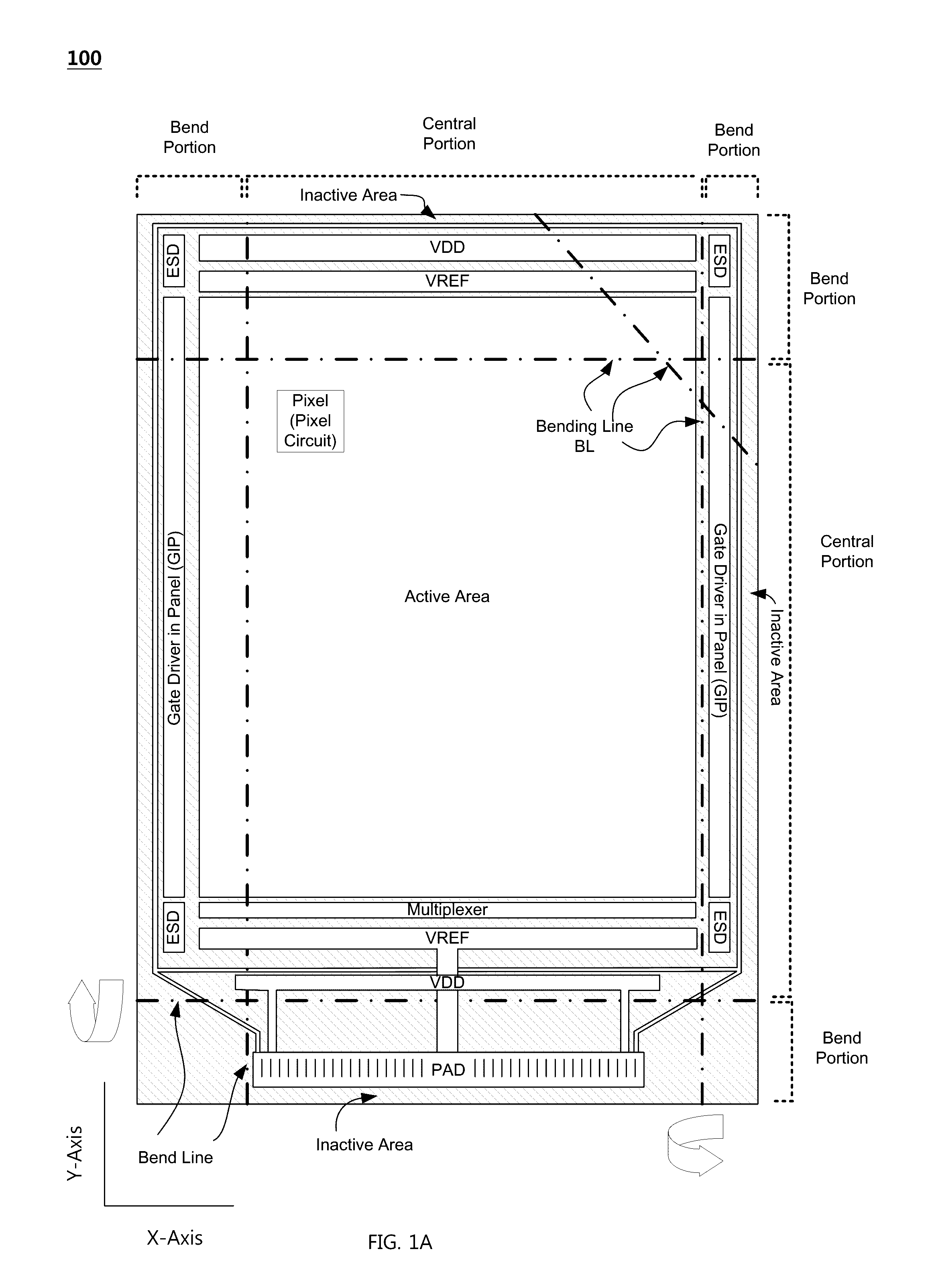
[0030]FIGS. 1A-1C illustrate exemplary flexible display 100 which may be incorporated in electronic devices. Referring to FIG. 1A, the flexible display 100 includes at least one active area (i.e., display area), in which an array of display pixels are formed therein. One or more inactive areas may be provided at the periphery of the active area. That is, the inactive area may be adjacent to one or more sides of the active area. In FIG. 1A, the inactive area surrounds a rectangular shape active area. However, it should be appreciated that the shapes of the active area and the arrangement of the inactive area adjacent to the active area are not particularly limited as the exemplary flexible display 100 illustrated in FIG. 1A. The active area and the inactive area may be in any shape suitable to the design of the electronic device employing the flexible display 100. Non-limiting examples of the active area shapes in the flexible display 100 include a pentagonal shape, a hexagonal shape...


PUM

PropertyMeasurementUnit
bend angleaaaaaaaaaa
bend radiusaaaaaaaaaa
thicknessaaaaaaaaaa

Abstract

There is provided a flexible display having a plurality of innovations configured to allow bending of a portion or portions to reduce apparent border size and / or utilize the side surface of an assembled flexible display.

Description

BACKGROUND[0001]Technical Field[0002]This relates generally to electronic devices, and more particularly, to electronic devices with a display.[0003]Description of the Related Art[0004]Electronic devices often include displays. For example, cellular telephones and portable computers include displays for presenting information to a user. Components for the electronic device, including but not limited to a display, may be mounted in the housing made of plastic or metal.[0005]An assembled display may include a display panel and a number of components for providing a variety of functionalities. For instance, one or more display driving circuits for controlling the display panel may be included in a display assembly. Examples of the driving circuits include gate drivers, emission (source) drivers, power (VDD) routing, electrostatic discharge (ESD) circuits, multiplex (mux) circuits, data signal lines, cathode contacts, and other functional elements. There may be a number of peripheral ci...

Claims


Application Information

Patent Timeline
Patent Type & Authority Patents(United States)
IPC IPC(8): H05K1/00H05K1/02G02F1/1333H05K1/18G02F1/1345
CPCH05K1/028G02F1/13452G02F1/133305H05K1/189G02F2201/122H05K2201/09036G02F1/1345G02F1/13454H01L23/562H01L23/564H01L27/1218H01L27/1222H01L27/124G02F2201/50G02F1/13456H10K59/40H10K2102/311H10K59/873H10K59/8791G09F9/301Y02E10/549Y02P70/50H10K59/131H10K77/111H10K59/1213H10K59/87H05K1/0259H10K50/86H10K50/844
Inventor KWON, SEYEOULYANG, HEESEOKYOUN, SANGCHEON
Owner LG DISPLAY CO LTD
Why Eureka
Try Eureka