Semiconductor apparatus

a technology of semiconductor and apparatus, which is applied in the direction of semiconductor devices, electrical apparatus, basic electric elements, etc., can solve the problems of increasing on-resistance, increasing breakdown voltage, and inviting greater loss, so as to improve breakdown voltage, ease the intensity of surface electric field, and improve the effect of breakdown voltag

Active Publication Date: 2017-02-21
FUJI ELECTRIC CO LTD
View PDF43 Cites 2 Cited by
  • Summary
  • Abstract
  • Description
  • Claims
  • Application Information

AI Technical Summary

Benefits of technology

[0030]According to embodiments of the first aspect of the invention, because the third regions of the second conductivity are provided, the high electric field near the outermost active region is relaxed when positive charges (positive ions) are present between the first conductive layer and the second conductive layer. This suppresses the fluctuation of breakdown voltage caused by positive charges. Because the second conductive layer is provided, depletion layer expansion reaching the termination of the peripheral region is avoided when negative charges (negative ions) are present between the first conductive layer and the second conductive layer. This suppresses a drop in breakdown voltage caused by negative charges. Because the second parallel pn-layer is provided, the depletion layer easily expands in the peripheral region. Hence high breakdown voltage is achieved easily.
[0086]The semiconductor apparatus, as described for embodiments of the present invention, offers an effect of improving robustness against charges on breakdown voltage.

Problems solved by technology

The portion serving as the high-resistance n−-drift layer, however, is depleted of carriers in the off-state, increasing breakdown voltage.
Conversely, a semiconductor apparatus with high breakdown voltage has a thicker n−-drift layer, which increases on-resistance, inviting greater loss.
A lack of the peripheral structure results in a drop in breakdown voltage at the termination of a drift layer, which makes achieving high breakdown voltage difficult.
A semiconductor apparatus having low robustness against charges manages to secure initial breakdown voltage but gradually loses its breakdown voltage as time elapses, which poses a problem of difficulty in ensuring breakdown voltage reliability.
For example, the semiconductor apparatus disclosed in the Patent Document 5 has no parallel pn-layer under an n−-layer of the peripheral structure, which poses a problem of difficulty in achieving high breakdown voltage.
The semiconductor apparatus disclosed in the Patent Document 6 has no n−-layer on the surface of the peripheral structure, which poses a problem that securing breakdown voltage is difficult when negative charges are present at the surface of the peripheral structure.
The semiconductor apparatus disclosed in the Patent Document 7 poses a problem that electric field concentration occurs at a stopper electrode, deteriorating breakdown voltage when negative charges are present at the surface of the peripheral structure.
The semiconductor apparatus disclosed in the Patent Document 8 poses a problem that with the termination working actually as the second-conductive (p-type) termination, charge imbalance toward the second-conductive type (p-type) causes the breakdown voltage of the peripheral region to become lower than that of the active region.
As depicted in FIG. 54, the presence of positive charges (positive ions) on an oxide film between a field plate electrode and a channel stopper electrode results in a drop in breakdown voltage.
The presence of positive charges (positive ions) on the oxide film of the peripheral region, however, makes expansion of the depletion layer difficult, thus causing an electric field at the field plate end to intensify.
As a result, breakdown voltage drops.
This leads to a drop in breakdown voltage.
At the pitch transition of the parallel pn-layers, a drop in breakdown voltage due to charge imbalance easily occurs.
This leads to a drop in breakdown voltage.

Method used


Image

  • Semiconductor apparatus
  • Semiconductor apparatus
  • Semiconductor apparatus

Examples


first embodiment

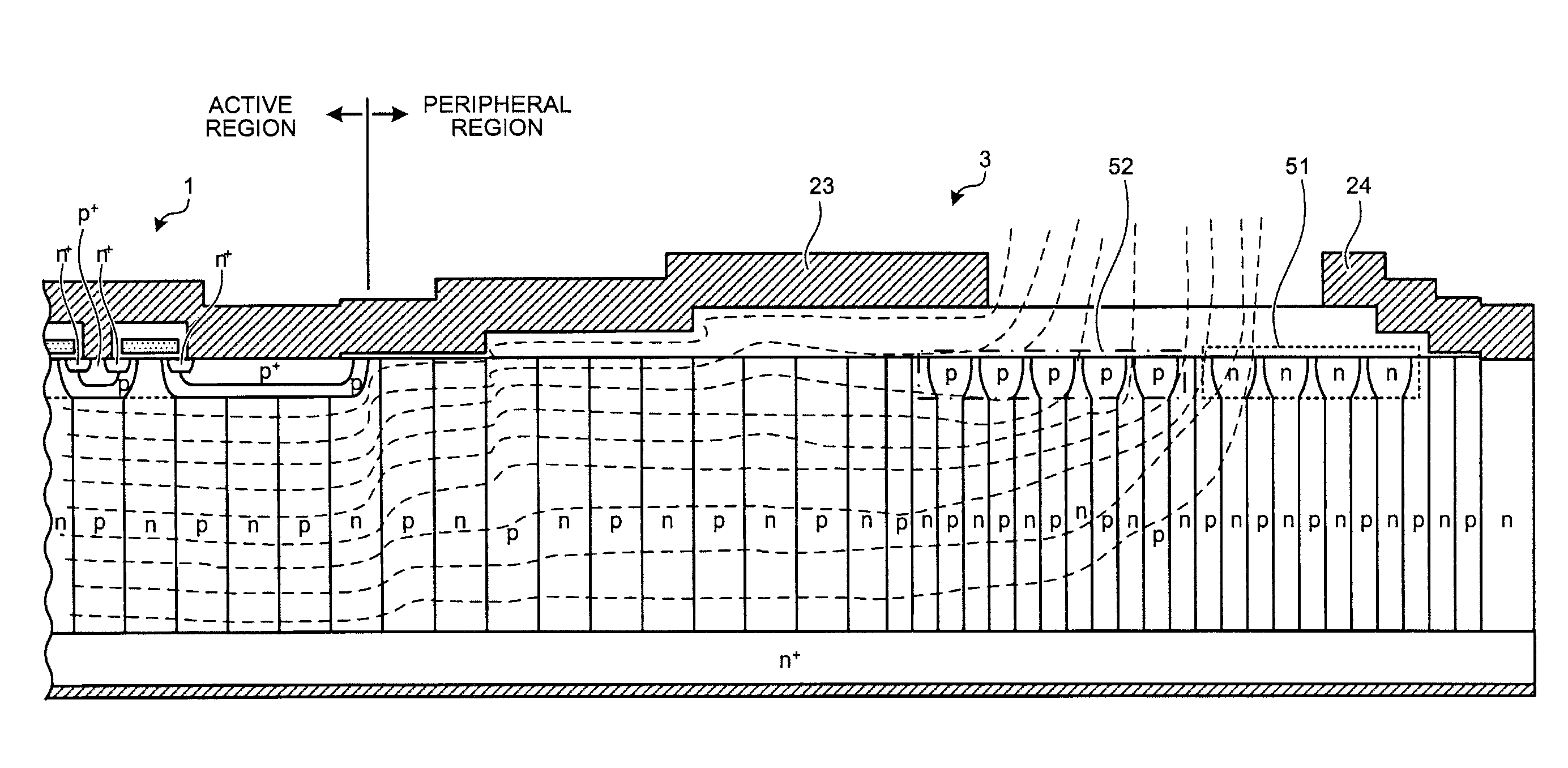
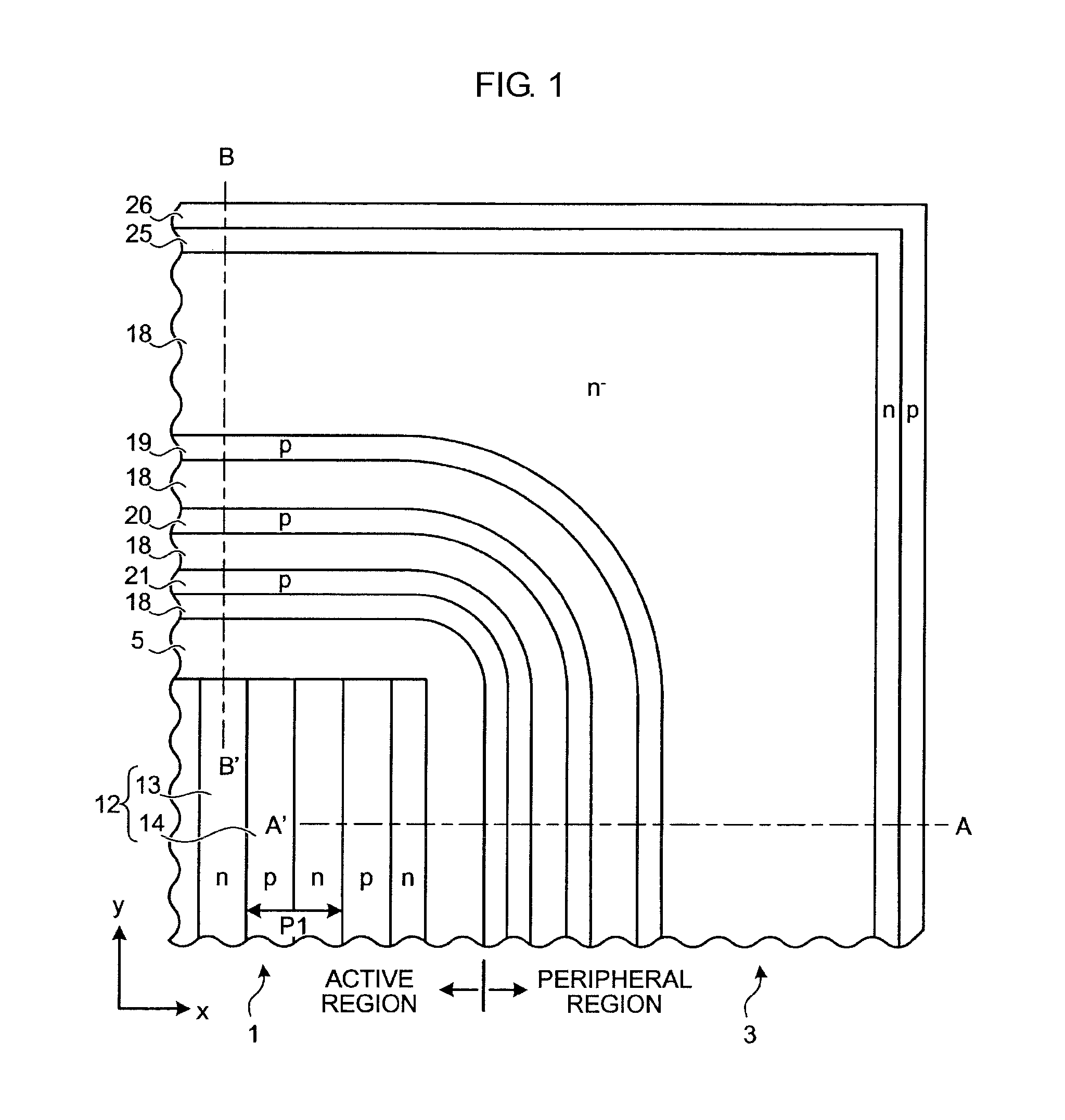
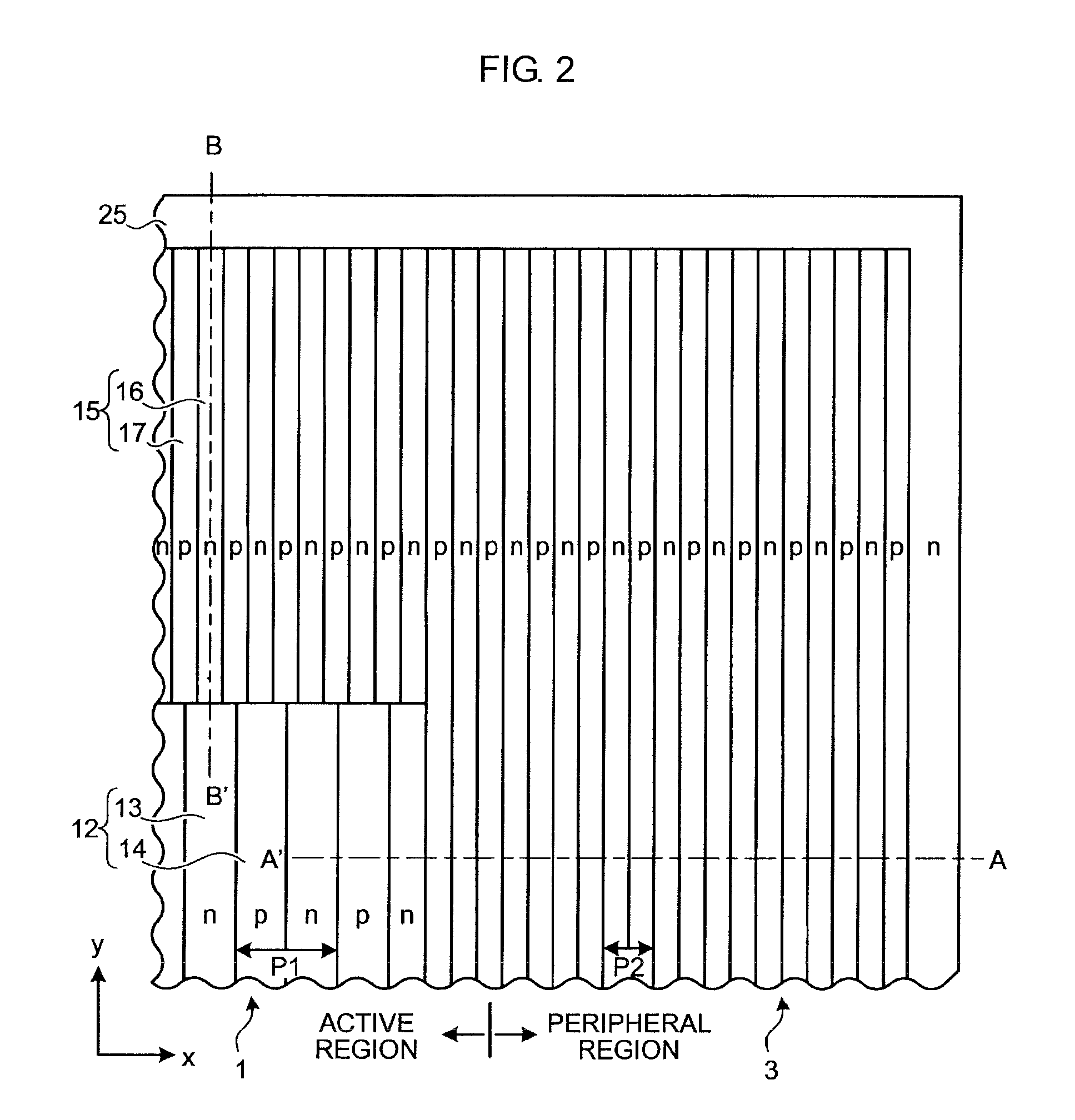
[0145]FIG. 1 is a top view of a semiconductor apparatus of a first embodiment. FIG. 2 is a horizontal sectional view of the semiconductor apparatus of the first embodiment. FIG. 3 is a vertical sectional view along an A-A′ line in FIG. 1 of the semiconductor apparatus of the first embodiment. FIG. 4 is a vertical sectional view along a B-B′ line in FIG. 1 of the semiconductor apparatus of the first embodiment. FIGS. 1 and 2 depict one-fourth of the semiconductor apparatus (FIGS. 5, 6, 13, 14, 27, 34, 37, 38, and 43 to 53 depict the same). FIG. 1 depicts the respective shapes of a parallel pn-layer, an n-channel stopper region, a p-base region at the outermost location of the active region, and p-guard ring regions at a first main surface (FIGS. 5 and 13 depict the same). FIG. 2 depicts shapes along a section that crosses the parallel pn-layer at both active region and peripheral region, for example, shapes along a section at a depth half of the parallel pn-layer of the active region...

second embodiment

[0152]FIG. 5 is a top view of a semiconductor apparatus of a second embodiment. FIG. 6 is a horizontal sectional view of the semiconductor apparatus of the second embodiment. FIG. 7 is a vertical sectional view along an A-A′ line in FIG. 5 of the semiconductor apparatus of the first embodiment. FIG. 8 is a vertical sectional view along a B-B′ line in FIG. 5 of the semiconductor apparatus of the second embodiment. As depicted in FIGS. 5 to 8, the second embodiment is different from the first embodiment in the following two respects. One respect is that the pitch transition of the parallel pn-layers, i.e., the boundary between the first parallel pn-layer 12 and the second parallel pn-layer 15 is under the n−-surface region 18. The other respect is that the p-guard ring regions 19, 20, and 21 are connected electrically to field plate electrodes 23, 27, and 28, respectively. The field plate electrodes 23, 27, and 28 are formed to extend over each of the p-guard ring regions 19, 20, and ...

third embodiment

[0156]FIG. 13 is a top view of a semiconductor apparatus according to a third embodiment. FIG. 14 is a horizontal sectional view of the semiconductor apparatus according to the third embodiment. FIG. 15 is a vertical sectional view along an A-A′ line in FIG. 13 of the semiconductor apparatus according to the third embodiment. FIG. 16 is a vertical sectional view along a B-B′ line in FIG. 13 of the semiconductor apparatus according to the third embodiment. As depicted in FIGS. 13 to 16, the third embodiment is different from the second embodiment in that the direction of the stripes of the second parallel pn-layer 15 is different from the direction of the stripes of the first parallel pn-layer 12. For example, the direction of the stripes of the second parallel pn-layer 15 may be perpendicular to the direction of the stripes of the first parallel pn-layer 12. In other configurative aspects, the third embodiment is substantially identical to the second embodiment.

[0157]The third embod...


PUM


Abstract

A semiconductor apparatus that has a first parallel pn-layer formed between an active region and an n+-drain region. A peripheral region is provided with a second parallel pn-layer, which has a repetition pitch narrower than the repetition pitch of the first parallel pn-layer. An n−-surface region is formed between the second parallel pn-layer and a first main surface. On the first main surface side of the n−-surface region, a plurality of p-guard ring regions are formed to be separated from each other. A field plate electrode is connected electrically to the outermost p-guard ring region among the p-guard ring regions. A channel stopper electrode is connected electrically to an outermost peripheral p-region of the peripheral region.

Description

CROSS-REFERENCE TO RELATED APPLICATIONS[0001]This application is a continuation application, filed under 35 U.S.C. §111(a), of International Application No. PCT / JP2010 / 004825, filed Jul. 29, 2010, which claimed priority to Japanese Application No. 2009-180131, filed Jul. 31, 2009, the entire contents of which are incorporated herein by reference.BACKGROUND[0002]1. Field[0003]This invention relates to a semiconductor apparatus that is applicable to an active element, such as a MOSFET (Metal Oxide Semiconductor Field Effect Transistor), an IGBT (Insulated Gate Bipolar Transistor), and a bipolar transistor, and to a passive element, such as a diode, and that which can achieve both higher breakdown voltage and higher current capacity.[0004]2. Description of Related Art[0005]In general, a semiconductor apparatus is classified as a horizontal element having an electrode formed on one surface of a semiconductor substrate or as a vertical element having electrodes on both surfaces of a semi...

Claims


Application Information

Patent Timeline
Patent Type & Authority Patents(United States)
IPC IPC(8): H01L29/78H01L29/08H01L29/40H01L29/417H01L29/06
CPCH01L29/7811H01L29/0634H01L29/0878H01L29/0619H01L29/0638H01L29/0696H01L29/402H01L29/404H01L29/41741
Inventor ONISHI, YASUHIKOSUGI, AKIO
Owner FUJI ELECTRIC CO LTD
Why Eureka
Try Eureka