RF impedance matching network

a technology of impedance matching and impedance matching, which is applied in the direction of resistance/reactance/impedence, multiple-port network, instruments, etc., can solve the problems of unstable fabrication process parameters, small feature geometries, and easy mechanical failure of vvc devices

Active Publication Date: 2017-02-28
ASM AMERICA INC
View PDF187 Cites 56 Cited by
  • Summary
  • Abstract
  • Description
  • Claims
  • Application Information

AI Technical Summary

Benefits of technology

The present invention provides an improved impedance matching network for use in semiconductor fabrication systems and processes. The network includes a transformation circuit that provides a transformed impedance that is less than the fixed source impedance, and two shunt circuits with variable components that provide capacitance or inductance to match the load impedance. The network can be controlled through a control signal to adjust the capacitance values of the shunt circuits and create an impedance match at the RF input. The technical effects of this invention include improved efficiency and accuracy in semiconductor fabrication processes.

Problems solved by technology

The VVC is an electromechanical device prone to mechanical failures.
As semiconductor devices shrink in size and become more complex, the feature geometries become very small.
During a significant amount of the matching process, which includes the microprocessor and FPGA determining the capacitances for the VVCs needed to create the match, controlling the VVCs to the achieve the determined capacitances, and then finally time for the RF matching network circuits to stabilize with the new capacitances, the fabrication process parameters are unstable, and these unstable process parameters must be accounted for as pan of the overall fabrication process.
Because the matching process time is becoming a more and more significant part of the time for each fabrication process step, the period in which process parameters are unstable becomes more of a factor in the overall fabrication process.
Further, matching networks employing EVCs often have drawbacks, including difficulty handling the voltage stresses that occur in high-power applications.

Method used


Image

  • RF impedance matching network
  • RF impedance matching network
  • RF impedance matching network

Examples


first embodiment

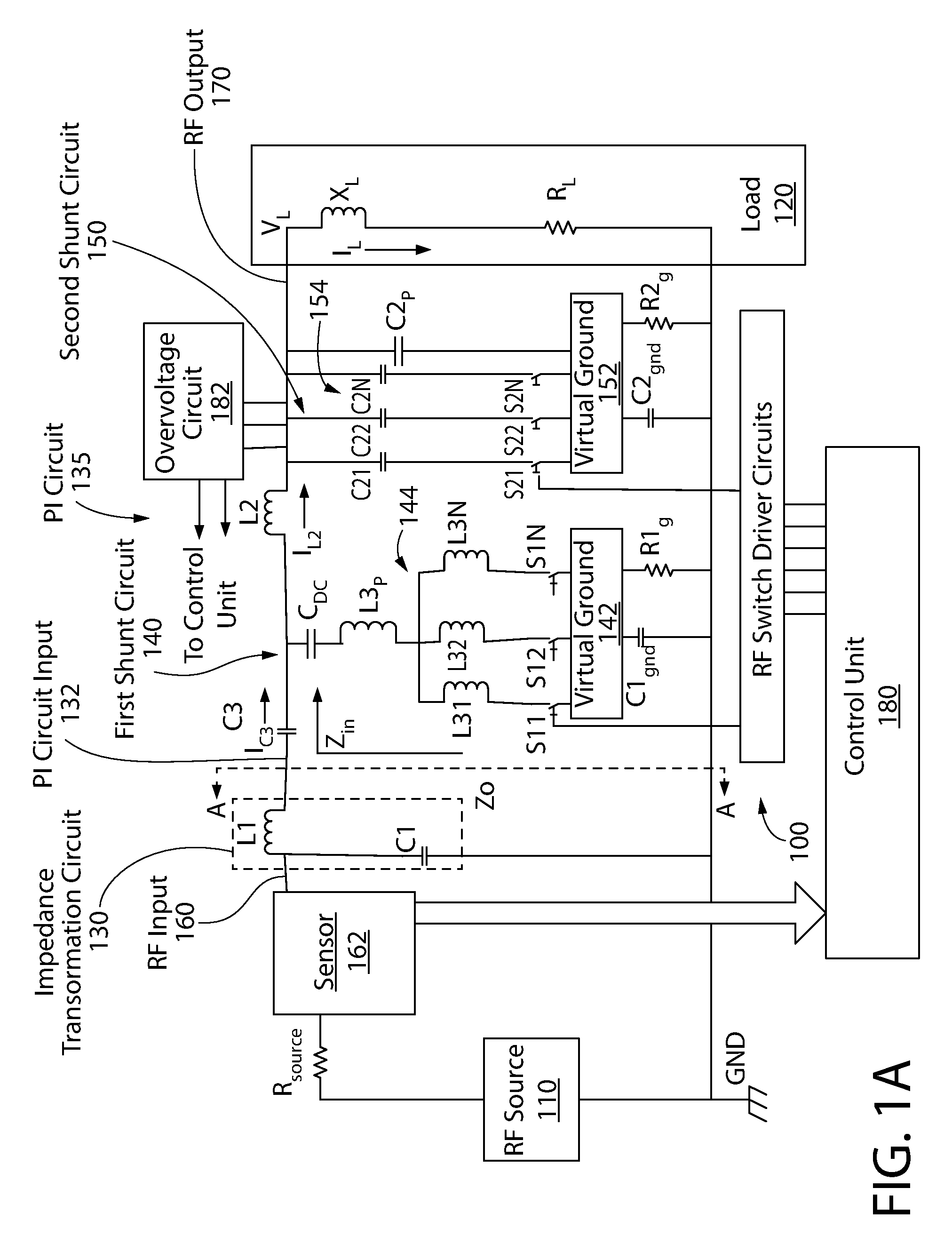
[0031]Turning in detail to the drawings, FIG. 1A illustrates an RF impedance matching network 100 according to the invention. The matching network 100 includes an RF input 160 configured to couple to an RF source 110, and an RF output 170 coupled to a load 120. A sensor 162 is coupled at the RF input 160 between the RF source 110 and the matching network 100. In the exemplified embodiment; the load 120 is a plasma chamber for semiconductor device fabrication. The semiconductor device can be microprocessor, a memory chip, or another type of integrated circuit or device. In other embodiments, the load 120 can be any load of variable impedance that can utilize an RF matching network.

[0032]In the exemplified embodiment, the RF impedance matching network 100 serves to help maximize the amount of RF power transferred from the RF source 110 to the plasma chamber 120 by matching the impedance at the RF input 160 to the fixed impedance of the RF source 110. The matching network 100 can consi...

second embodiment

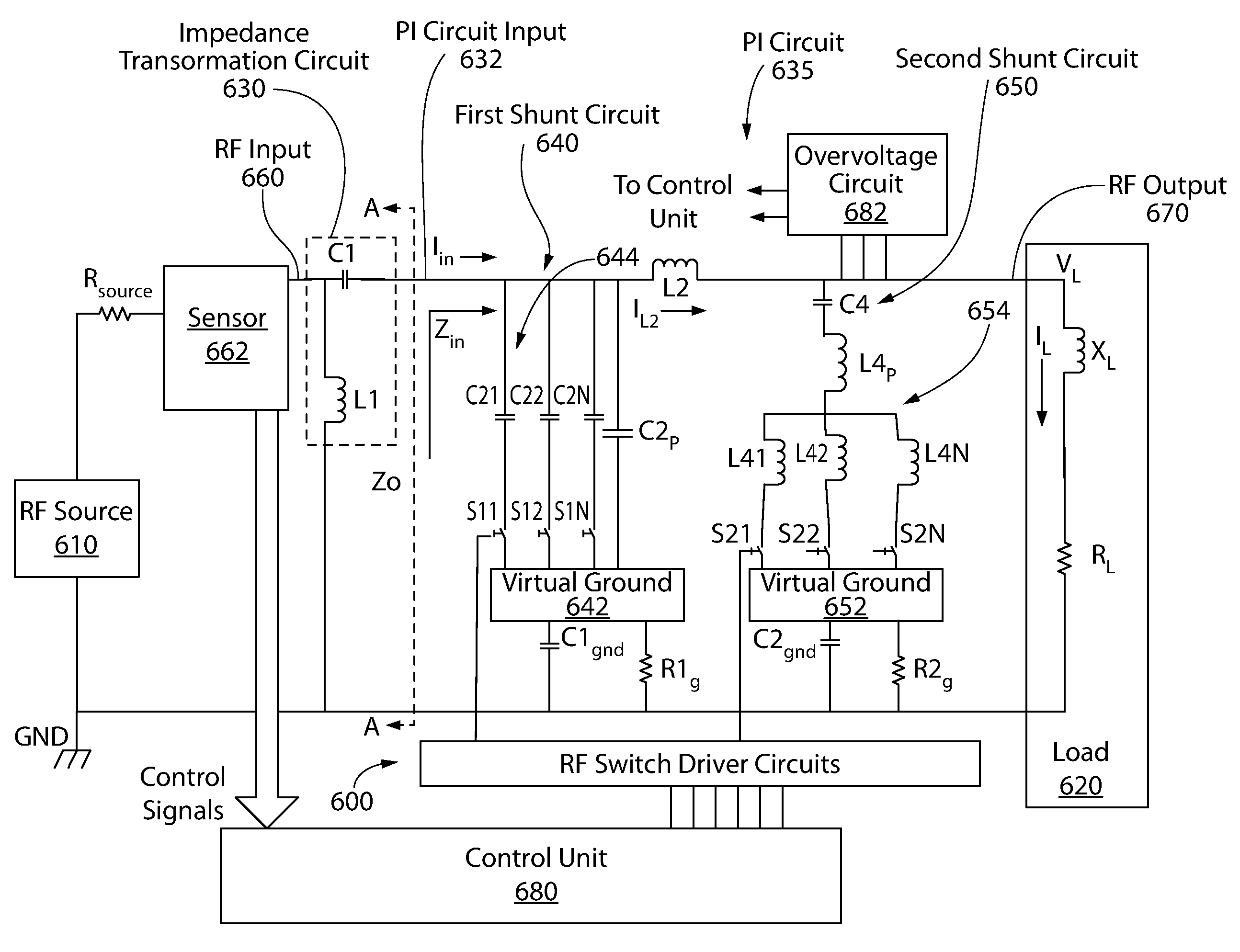
[0065]FIG. 2 is a schematic representation of an RF impedance matching, network 200. As will be described, this embodiment uses variable capacitance components 244, 254 in both shunt legs. As in FIG. 1A, the matching network 200 includes an RF input 260 configured to couple to an RF source 210 and an RF output 170 configured to couple to a load 220, a transformation circuit 230, and a PI circuit 235.

[0066]The transformation circuit 230 is again coupled to the RF input 260 and configured to provide a transformed impedance that is less than the fixed source impedance. The transformation capacitor C1, however, is in series with the RF input 260, and the transformation inductor L1 is in parallel to the RF input and coupled to the chassis ground GND.

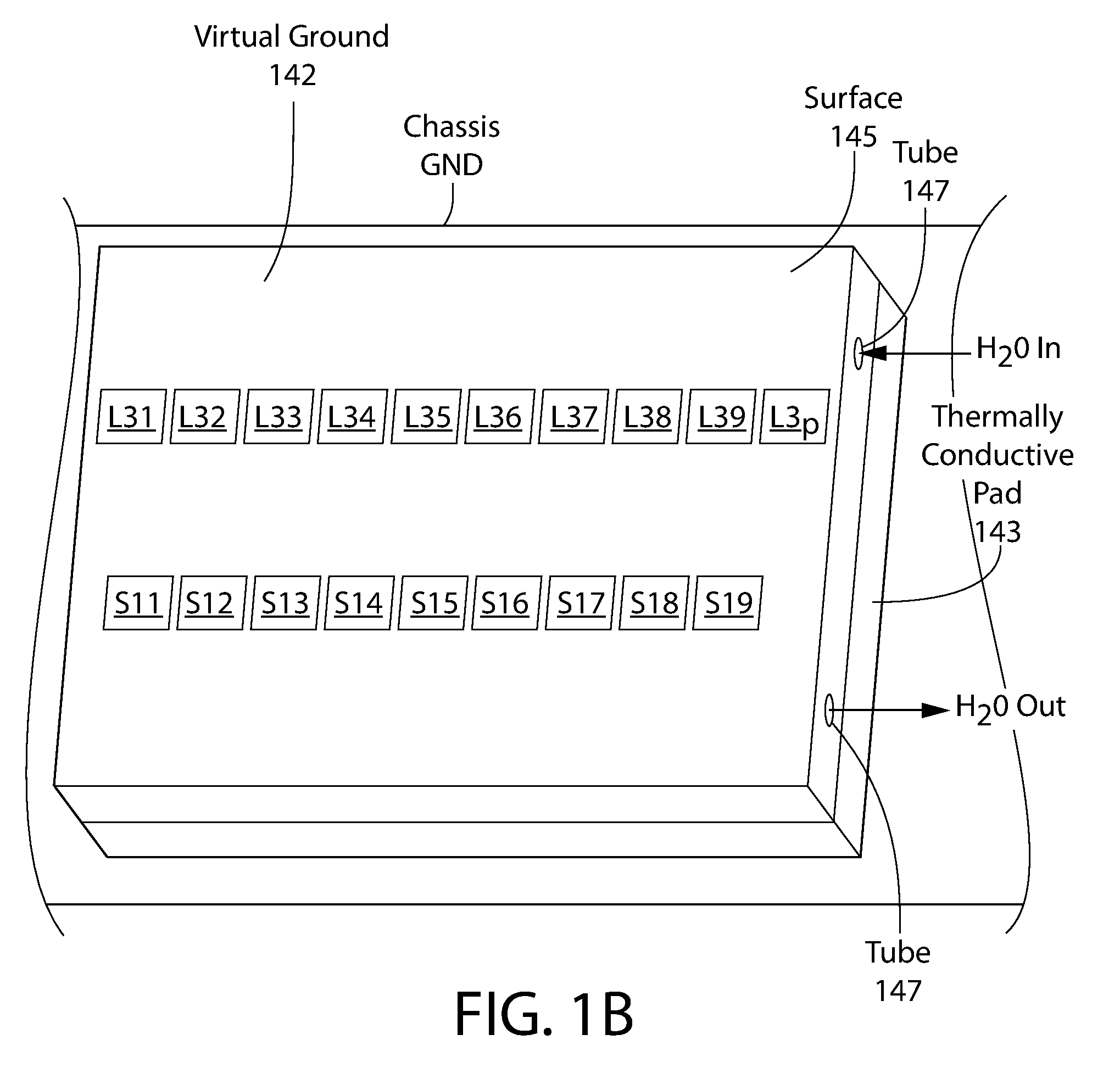
[0067]The first shunt circuit 240 is in parallel to the RF input 260. The circuit 240 includes a first shunt variable capacitance component 244 comprising (a) a plurality of first shunt capacitors C11, C12, C1N coupled in parallel, and (b) a ...

third embodiment

[0070]FIG. 3 is a schematic representation of an RF impedance matching network 300. In this embodiment, variable inductors 344, 354 are used in both shunt legs. As in the previous figures, the matching network 300 includes an RF input 360 configured to couple to an RF source 310 and an RF output 370 configured to couple to a load 320, a transformation circuit 330, and a PI circuit 335.

[0071]Similar to the embodiment shown in FIG. 1A, the transformation inductor L is in series with the RF input 360, and the transformation capacitor C1 is in parallel to the RF input 360 and coupled to a chassis ground GND. Also similar to FIG. 1A, the first shunt circuit 340 includes a first shunt padding, inductor L3P; a plurality of first shunt inductors L31, L32, L3N coupled in parallel to the first shunt padding inductor L3P; a plurality of first shunt switches S11, S12, S1N coupled to the plurality of first shunt inductors L31, L32, L3N and configured to connect and disconnect each of the plurali...


PUM


Abstract

An RF impedance matching network includes a transformation circuit coupled to an RF input and configured to provide a transformed impedance that is less than a fixed source impedance; a first shunt circuit in parallel to the RF input, the first shunt circuit including a first shunt variable component providing a first variable capacitance or inductance; and a first virtual ground coupled to the first shunt variable component and a ground; and a second shunt circuit in parallel to the RF input and, the second shunt circuit including a second shunt variable component providing a second variable capacitance or inductance; and a second virtual ground coupled to the second shunt variable component and the ground.

Description

CROSS REFERENCE TO RELATED APPLICATIONS[0001]The present application is a continuation of U.S. patent application Ser. No. 14 / 734,053, filed Jun. 9, 2015 which claims the benefit of U.S. Provisional Patent Application Ser. No. 62 / 118,552, filed Feb. 20, 2015, the disclosures of which are incorporated herein by reference in their entirety.FIELD OF THE INVENTION[0002]The field of the present invention relates to systems and methods for providing an RF impedance matching network.BACKGROUND OF THE INVENTION[0003]Semiconductor devices can include microprocessors, memory chips, and other types of integrated circuits and devices. The semiconductor device fabrication process uses plasma processing at different stages of the process. Plasma processing involves energizing a gas mixture by imparting energy to the gas molecules by introducing RF (radio frequency) energy into the gas mixture. This gas mixture is typically contained in a vacuum chamber, referred to as a plasma chamber, and the RF...

Claims


Application Information

Patent Timeline
Patent Type & Authority Patents(United States)
IPC IPC(8): H03H7/40G01R27/28H01L21/3065G01R27/26H03H7/38H01L21/311H01J37/32H01L21/3213H01L21/02H01L21/285H01L21/67
CPCH03H7/38G01R27/2605G01R27/28H01J37/32183H01L21/02274H01L21/28556H01L21/3065H01L21/31116H01L21/31138H01L21/32136H01L21/67115H03H7/40
Inventor MAVRETIC, ANTON
Owner ASM AMERICA INC
Why Eureka
Try Eureka