GOA circuit and liquid crystal display

a liquid crystal display and circuit technology, applied in static indicating devices, cathode-ray tube indicators, instruments, etc., can solve the problems of increasing the design difficulty of ltps goa circuits, low yield rate of ltps displays, and many scanning-driving circuits applied for amorphous silicon semiconductors may not be applied easily to ltps tft-lcd, etc., to achieve the effect of reducing the delay of output signals

Active Publication Date: 2017-03-07
TCL CHINA STAR OPTOELECTRONICS TECH CO LTD +1
View PDF1 Cites 1 Cited by
  • Summary
  • Abstract
  • Description
  • Claims
  • Application Information

AI Technical Summary

Benefits of technology

[0018]Distinguishing from the current technology, the beneficial effects of the present disclosure is that two clock signals having different pulse widths are input to the N-staged pull-up circuits and the N-staged transfer circuits such that the output signals may be separated from the transfer signals. Therefore, the voltage level of Q(N) point is raised to a better high voltage level. The delay of the output signals is reduced, and the better charge of the scanning lines in the GOA circuit is ensured for facilitating the normal operation for each point in the circuit.

Problems solved by technology

However, the low yield rate for LTPS displays has greatly perplexed the panel manufactures.
This increases the difficulty on the design of the LTPS GOA circuit.
Many scanning-driving circuits applied for amorphous silicon semiconductors may not be applied easily to LTPS TFT-LCD.
Some functional problems exist.
This would directly result in malfunction on the IGZO GOA circuit.

Method used


Image

  • GOA circuit and liquid crystal display
  • GOA circuit and liquid crystal display
  • GOA circuit and liquid crystal display

Examples


first embodiment

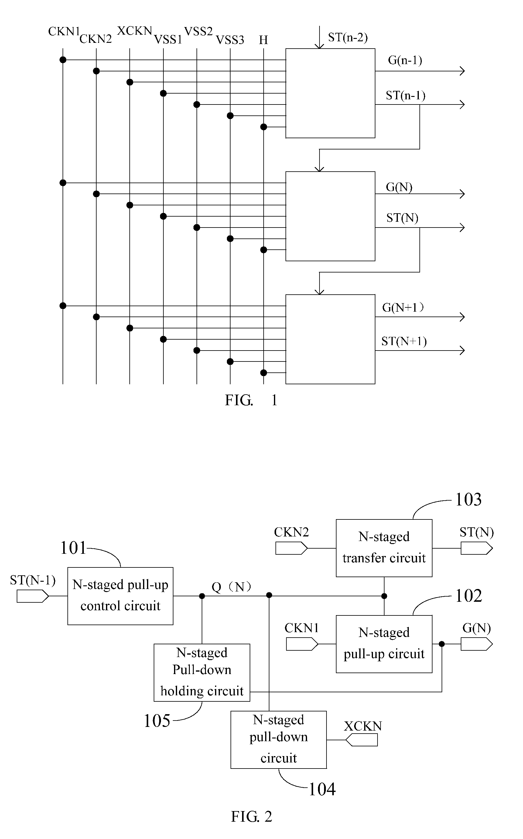
[0029]Refer to FIG. 1 for the schematic diagram of the cascading GOA units of the GOA circuit according to the disclosure. The GOA circuit comprises a plurality of GOA units. The N-staged GOA units charge the Nth-staged horizontal scanning line G(N) in the display region.

[0030]Refer to FIG. 2 for the schematic diagram of the GOA unit of the first embodiment of the GOA circuit according to the disclosure.

[0031]The N-staged GOA units comprise N-staged pull-up control circuits 101, N-staged pull-up circuits 102, N-staged transfer circuits 103, N-staged pull-down circuits 104, and N-staged pull-down holding circuits 105. The N-staged pull-up circuits 102 and the N-staged pull-down holding circuits 105 connect to the Nth-staged gate signal point Q(N) and the Nth-staged horizontal scanning line G(N) respectively. The N-staged pull-up control circuits 101, the N-staged pull-down circuits 104, and the N-staged transfer circuits 103 connect to the Nth-staged gate signal point Q(N).

[0032]The ...

second embodiment

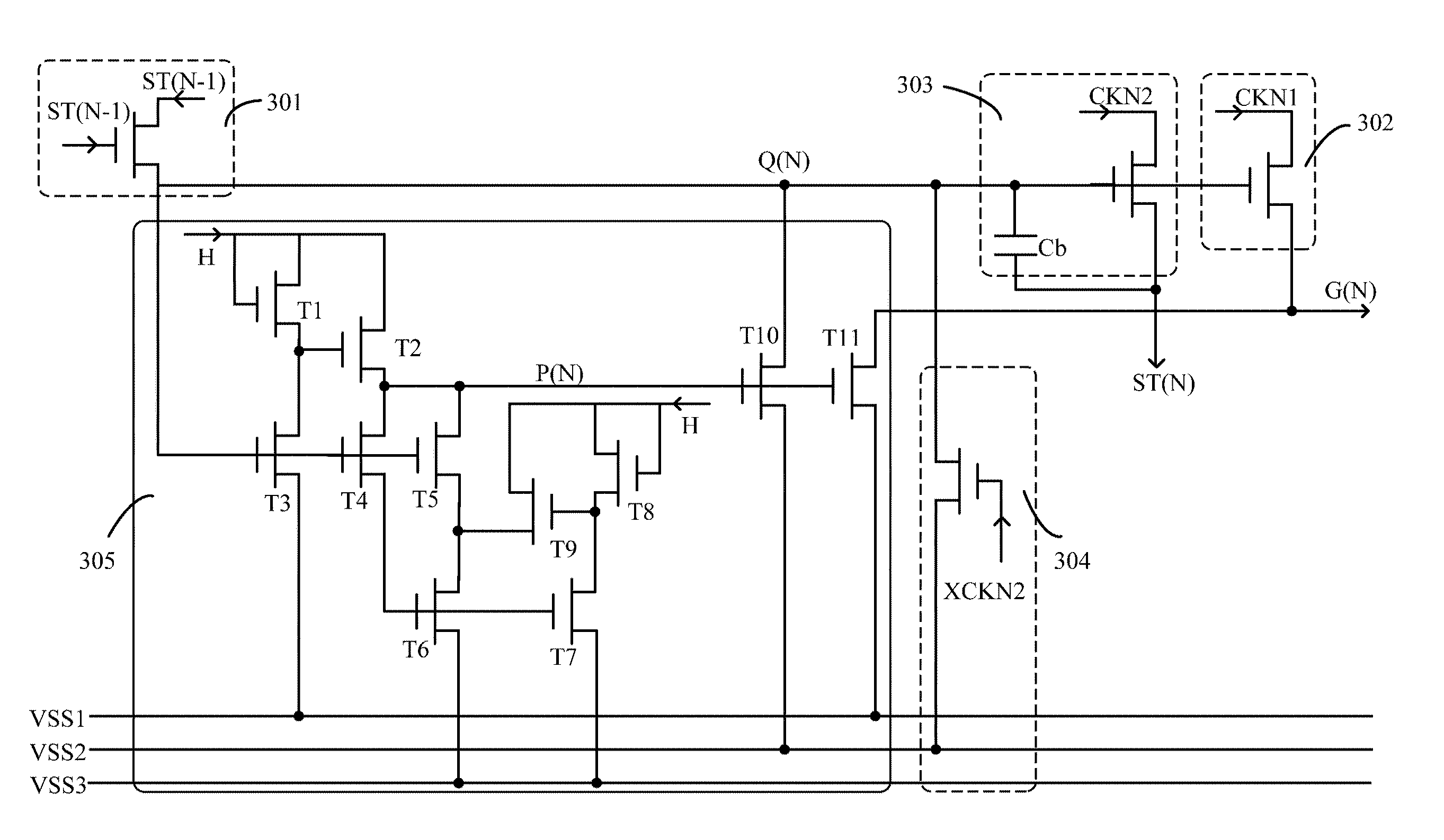
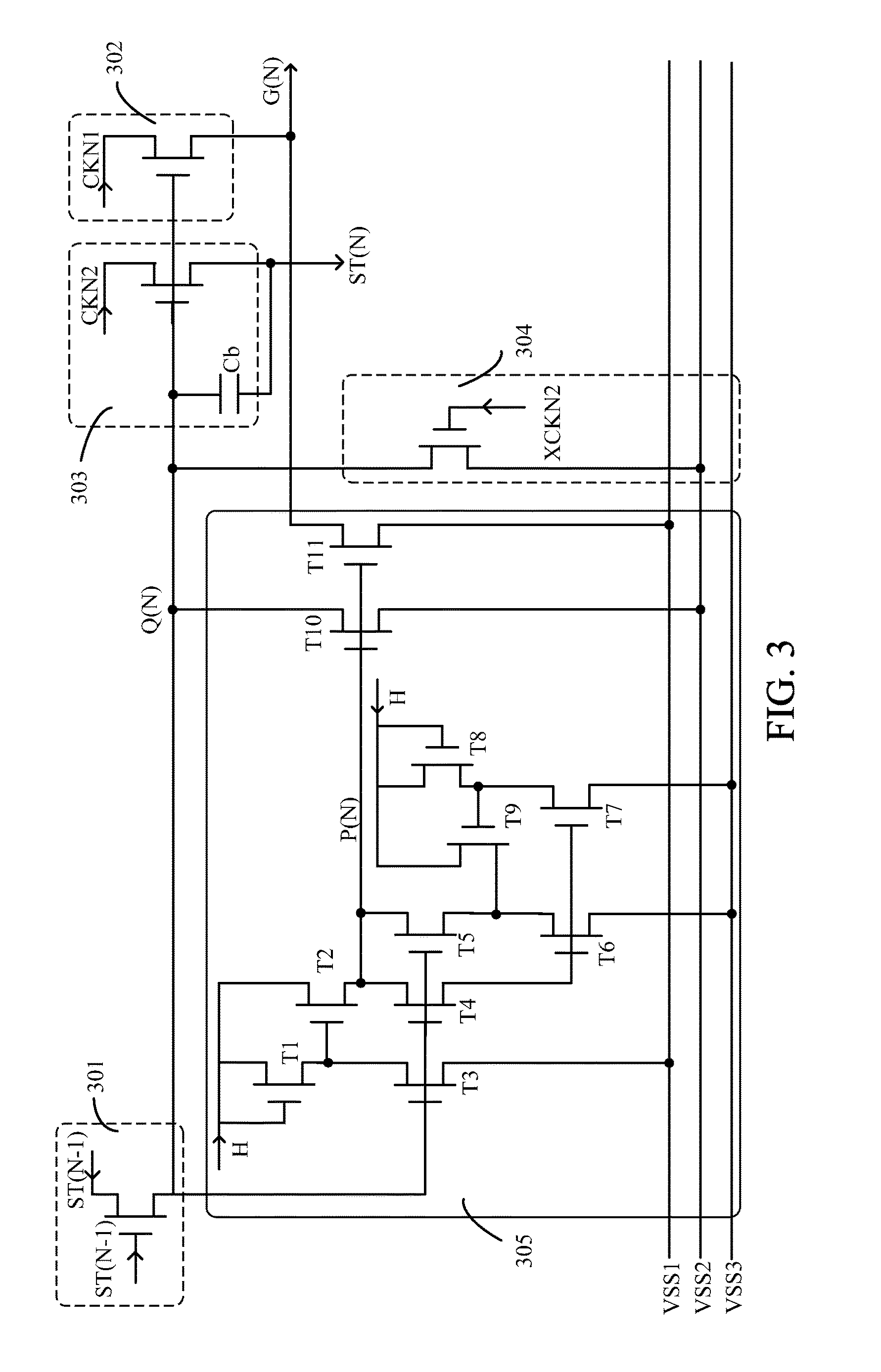
[0035]Refer to FIG. 3 for the schematic diagram illustrating the specific circuit connection of the GOA unit of the GOA circuit according to the disclosure. The N-staged GOA units comprise N-staged pull-up control circuits 301, N-staged pull-up circuits 302, N-staged transfer circuits 303, N-staged pull-down circuits 304, and N-staged pull-down holding circuits 305. The N-staged pull-up circuits 302 and the N-staged pull-down holding circuits 305 connect to the Nth-staged gate signal point Q(N) and the Nth-staged horizontal scanning line G(N) respectively. The N-staged pull-up control circuits 301, the N-staged pull-down circuits 304, and the N-staged transfer circuits 303 connect to the Nth-staged gate signal point Q(N). The N-staged pull-up circuits 302 and the N-staged transfer circuits turn on when Q(N) is at a high voltage level, and respectively receive a first clock signal CKN1 and a second clock signal CKN2 and output the signals. The pulse width of the second clock signal C...


PUM


Abstract

A GOA circuit comprising GOA units and a liquid crystal display are disclosed. The N-staged GOA units charge the Nth-staged horizontal scanning line in the display region, and comprise N-staged pull-up control circuits, N-staged pull-up circuits, N-staged transfer circuits, N-staged pull-down circuits, and N-staged pull-down holding circuits. The N-staged pull-up circuits turn on when the Nth-staged gate signal point is at a high voltage level, receive a first clock signal and charge the N-staged horizontal scanning lines when the first clock signal is at a high voltage level. The N-staged transfer circuits receive a second clock signal when the Nth-staged gate signal point is at the high voltage level and output N-staged transfer signals to control the operation of the (N+1)-staged GOA units. The disclosure may ensure the scanning lines in the GOA circuit to be better charged for facilitating normal operation for each point in the circuit.

Description

BACKGROUND[0001]Technical Field[0002]The disclosure is related to the technology field for the liquid crystal display, and more particular to a GOA circuit and a liquid crystal display.[0003]Related Art[0004]Among displays with small size and high resolution, it is known to the public that LTPS (Low Temperature Poly-Silicon) technology has been widely adopted due to the high mobility and stability. However, the low yield rate for LTPS displays has greatly perplexed the panel manufactures. In this respect, the array test is a necessary and prompt approach to monitor each manufacturing process.[0005]With the development of LTPS semi-conductor thin film transistors, due to the ultra-high carrier mobility of the LTPS semi-conductor thin film transistors, corresponding peripheral integrated circuits for panels have become the focus of everyone's attention. And a lot of people are devoted into the related technology research for System on Panel (SOP), and it gradually becomes a reality.[0...

Claims


Application Information

Patent Timeline
Patent Type & Authority Patents(United States)
IPC IPC(8): G09G5/00G09G3/20G09G3/36
CPCG09G3/3677G09G3/20G09G2310/0251G09G2310/0267G09G2310/0286G09G2310/06G09G2310/08G09G2330/021G09G3/36
Inventor XIAO, JUNCHENG
Owner TCL CHINA STAR OPTOELECTRONICS TECH CO LTD
Why Eureka
Try Eureka