Array substrate, display panel and display device

A technology of array substrates and substrate substrates, applied in static indicators, instruments, etc., can solve the problems of increased power consumption of shift register unit output delay gate drive circuits, increased clock signal delays, increased number of parasitic capacitances, etc.

Active Publication Date: 2017-11-07
BOE TECH GRP CO LTD +1
View PDF3 Cites 0 Cited by
  • Summary
  • Abstract
  • Description
  • Claims
  • Application Information

AI Technical Summary

Problems solved by technology

[0006] As the resolution required by large-scale displays becomes higher and higher, the number of clock signal lines required in the gate drive circuit also increases, so the increase in clock signal lines will cause the leads connected to the clock signal lines to be disconnected from them. The number of parasitic capacitances at the intersection of the clock signal lines increases, which in turn causes an increase in the delay of the clock signal, resulting in an increase in the output delay of the shift register unit and the power consumption of the gate drive circuit

Method used


Image

  • Array substrate, display panel and display device
  • Array substrate, display panel and display device
  • Array substrate, display panel and display device

Examples


Embodiment 1

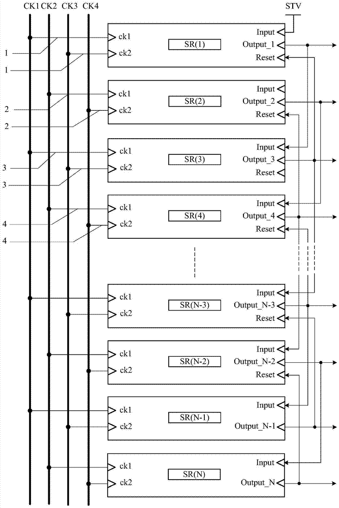
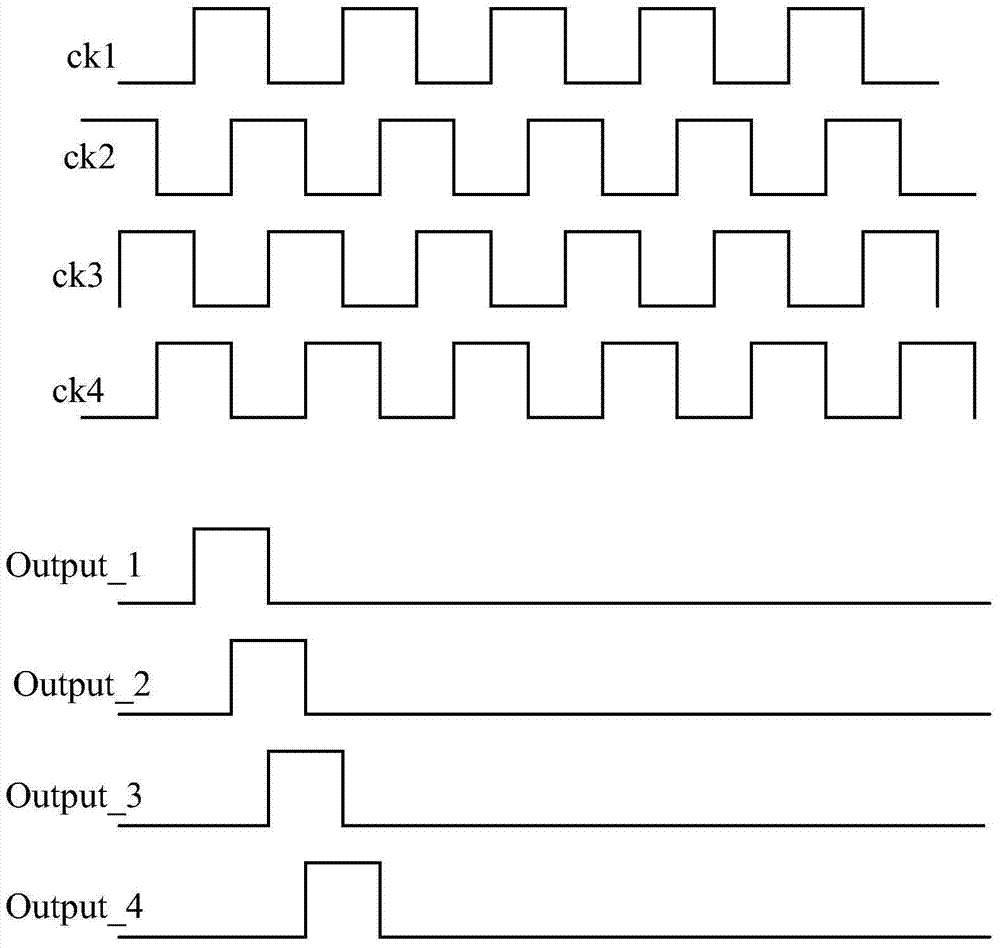
[0074] Take n equal to 2 as an example, such as Figure 3a As shown, it includes a base substrate (not shown in the figure), 2 sets of clock signal lines arranged side by side on the base substrate, and a set of clock signal lines (CK1, CK2, CK3 and CK4) on one side A gate drive circuit with a charging function; wherein the gate drive circuit includes cascaded multi-stage shift register units 1200 arranged side by side along the extension direction of the clock signal line, each of the shift register units has two clock signals The terminals 1201 are respectively used to receive clock signals with opposite phases, and the shift register units 1200 of each level correspond to a group of clock signal lines;

[0075] All the shift register units 1200 are divided into N shift register unit groups 12, for the kth shift register unit group 12, including the 4k-3 shift register unit 1200 to the 4k shift register unit 1200 ; Wherein, the shift register unit 1200 of the 4k-3 level to ...

Embodiment 2

[0084] Take n equal to 3 as an example, such as Figure 3b As shown, it includes a base substrate (not shown in the figure), 3 sets of clock signal lines arranged side by side on the base substrate, and 3 sets of clock signal lines (CK1, CK2, CK3, CK4, CK5 and CK6) A gate drive circuit with a pre-charging function on the side; wherein the gate drive circuit includes cascaded multi-stage shift register units 1200 arranged side by side along the extension direction of the clock signal line, each of which has The two clock signal terminals 1201 are respectively used to receive clock signals with opposite phases, and the shift register units 1200 of each level correspond to a group of clock signal lines;

[0085] All shift register units 1200 are divided into N shift register unit groups 12, for the kth shift register unit group 12, including the 6k-5th stage shift register unit 1200 to the 6kth stage shift register unit 1200 ; Wherein, the shift register unit 1200 of the 6k-5 le...

Embodiment 3

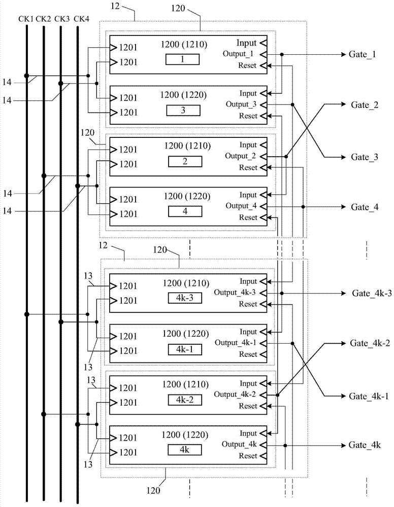
[0094] Take n equal to 2 as an example, such as Figure 3c As shown, it includes a base substrate (not shown in the figure), two sets of clock signal lines arranged side by side on the base substrate, and a gate with a pre-charge function on one side of the two sets of clock signal lines (CK1 and CK2). Pole drive circuit; wherein, the gate drive circuit includes cascaded multi-stage shift register units 1200 arranged side by side along the extension direction of the clock signal line, each of the shift register units has two clock signal terminals 1201 for Receiving clock signals with opposite phases and the shift register units 1200 at each level correspond to a group of clock signal lines;

[0095] For the kth shift register unit group 12, each adjacent two first-type shift register units 1210 and second-type shift register units 1220 are used as a subgroup 120, and two shift register units in each subgroup 120 The bit register unit 1200 corresponds to the same group of clo...


PUM


Abstract

The invention discloses an array substrate, a display panel, and a display device. Two adjacent shift register units of the first type and shift register units of the second type are used as a subgroup, and the two shift register units in each subgroup The signal ends of the shift register units used to connect to the same clock signal line are connected through the first lead, and the first lead is connected with the corresponding clock signal line through the second lead. In this way, by adjusting the arrangement sequence of the shift register units or reducing the number of clock signal lines, the overlap between the lead wires and the clock signal lines is reduced, thereby reducing the parasitic capacitance generated at the overlap between the lead wires and the clock signal lines. The number, thereby reducing the delay of the clock signal, and reducing the output delay of the shift register unit and the power consumption of the gate drive circuit.

Description

technical field [0001] The present invention relates to the field of display technology, in particular to an array substrate, a display panel and a display device. Background technique [0002] With the rapid development of display technology, displays show a development trend of high integration and low cost. Among them, the GOA (Gate Driver on Array, array substrate row driving) technology integrates the TFT (Thin Film Transistor, thin film transistor) gate switch circuit on the array substrate of the display panel to form a scan drive for the display panel, thus saving The bonding (Bonding) area of ​​the gate integrated circuit (IC, Integrated Circuit) and the wiring space of the fan-out (Fan-out) area can not only reduce the product cost in terms of material cost and manufacturing process, but also make the display panel Aesthetic design with symmetry on both sides and narrow frame; moreover, this integration process can also save the Bonding process in the direction of...

Claims


Application Information

Patent Timeline
Patent Type & Authority Patents(China)
IPC IPC(8): G09G3/20
Inventor 苏秋杰
Owner BOE TECH GRP CO LTD
Why Eureka
Try Eureka