
OLED driving compensation circuit and driving method thereof

a compensation circuit and driving mode technology, applied in the field of display technology, can solve problems such as uniform display of pixel units, and achieve the effects of avoiding the large width-length ratio of the third transistor, reducing the aperture ratio of pixel units, and reducing the area occupied by each pixel uni

Active Publication Date: 2017-03-07
BOE TECH GRP CO LTD
View PDF19 Cites 3 Cited by
  • Summary
  • Abstract
  • Description
  • Claims
  • Application Information

AI Technical Summary

Benefits of technology

[0007]The present invention aims to solve the above technical problems in the prior art and provide an OLED driving compensation circuit and a driving method thereof. Two electrodes of a driving transistor for generating driving current can be completely reset to respective initial voltage at a reset phase, so that a good compensation effect is obtained. Meanwhile, a width-length ratio of a transistor in an external compensation module can be further reduced, so that an aperture ratio of pixel units is improved and an area occupied by each pixel unit is reduced.
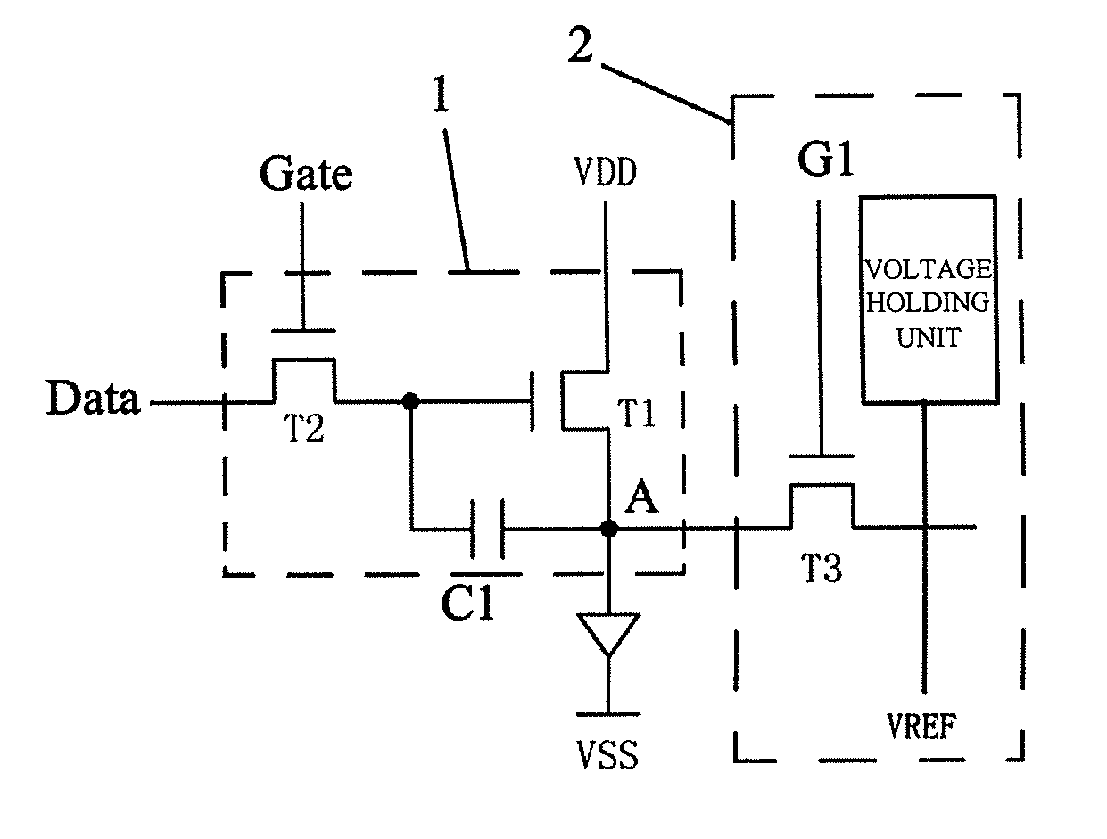
[0020]In the OLED driving compensation circuit provided by the embodiment of the present invention, the external compensation module compensates the voltages of the control electrode of the driving transistor and the electrode of the driving transistor connected with the second terminal of the storage capacitor, to avoid that the threshold voltage of the driving transistor, the voltage drop on the power line and the non-uniformity of film thickness in the OLEDs influence the luminance uniformity of each OLED in a frame of picture and the luminance uniformity of the OLEDs. Moreover, at the reset phase of compensation, the first voltage input by the power supply voltage terminal is equal to the reference voltage, so that the voltage on the electrode of the driving transistor connected with the second terminal of the storage capacitor is completely equal to the reference voltage, and then a best reset effect is achieved. Meanwhile, it is not needed to require the resistance of the third transistor to be further lower than that of the driving transistor in order that the difference between the voltage on the electrode of the driving transistor connected with the second terminal of the storage capacitor and the reference voltage is as small as possible, so that large width-length ratio of the third transistor can be avoided, and the problems that the aperture ratio of pixel units is reduced and the area occupied by each pixel unit is enlarged are avoided.
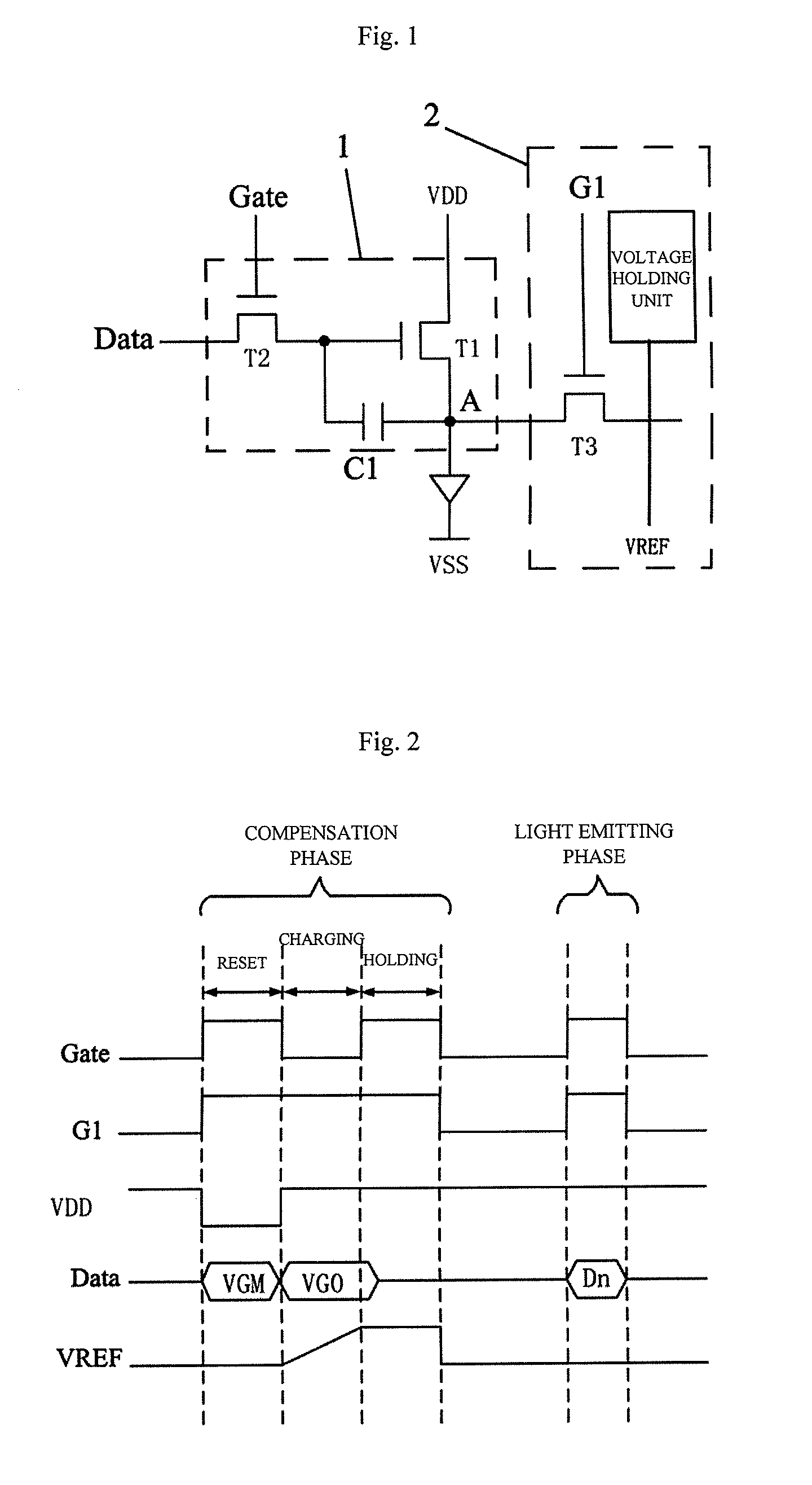
[0021]In the driving method for the OLED driving compensation circuit provided by the present invention, when the voltages of the control electrode of the driving transistor and the electrode connected with the second terminal of the storage capacitor are reset, the first voltage equal to the reference voltage is input to the power supply voltage terminal, and the reference voltage is also input to the reference voltage terminal, so that the voltage on the electrode of the driving transistor connected with the second terminal of the storage capacitor is equal to the reference voltage, and then a best reset effect can be achieved. Meanwhile, it is not needed to require the resistance of the third transistor to be further lower than that of the driving transistor in order that the difference between the voltage on the electrode of the driving transistor connected with the second terminal of the storage capacitor and the reference voltage is as small as possible, so that large width-length ratio of the third transistor can be avoided, and the problems that the aperture ratio of pixel units is reduced and the area occupied by each pixel unit is enlarged are avoided.

Problems solved by technology

Moreover, in the evaporation process of fabricating process for the OLED device, the thickness of film formed by evaporation has certain differences among different OLED devices, and the non-uniformity of the film thickness in the OLED devices also influences the display uniformity of the pixel units.

Method used


Image

  • OLED driving compensation circuit and driving method thereof
  • OLED driving compensation circuit and driving method thereof
  • OLED driving compensation circuit and driving method thereof

Examples


Embodiment Construction

[0028]The specific embodiments of the present invention will be described in detail below in combination with the accompanying drawings. It should be understood that the specific embodiments described herein are merely used for describing and interpreting the present invention, rather than limiting the present invention.

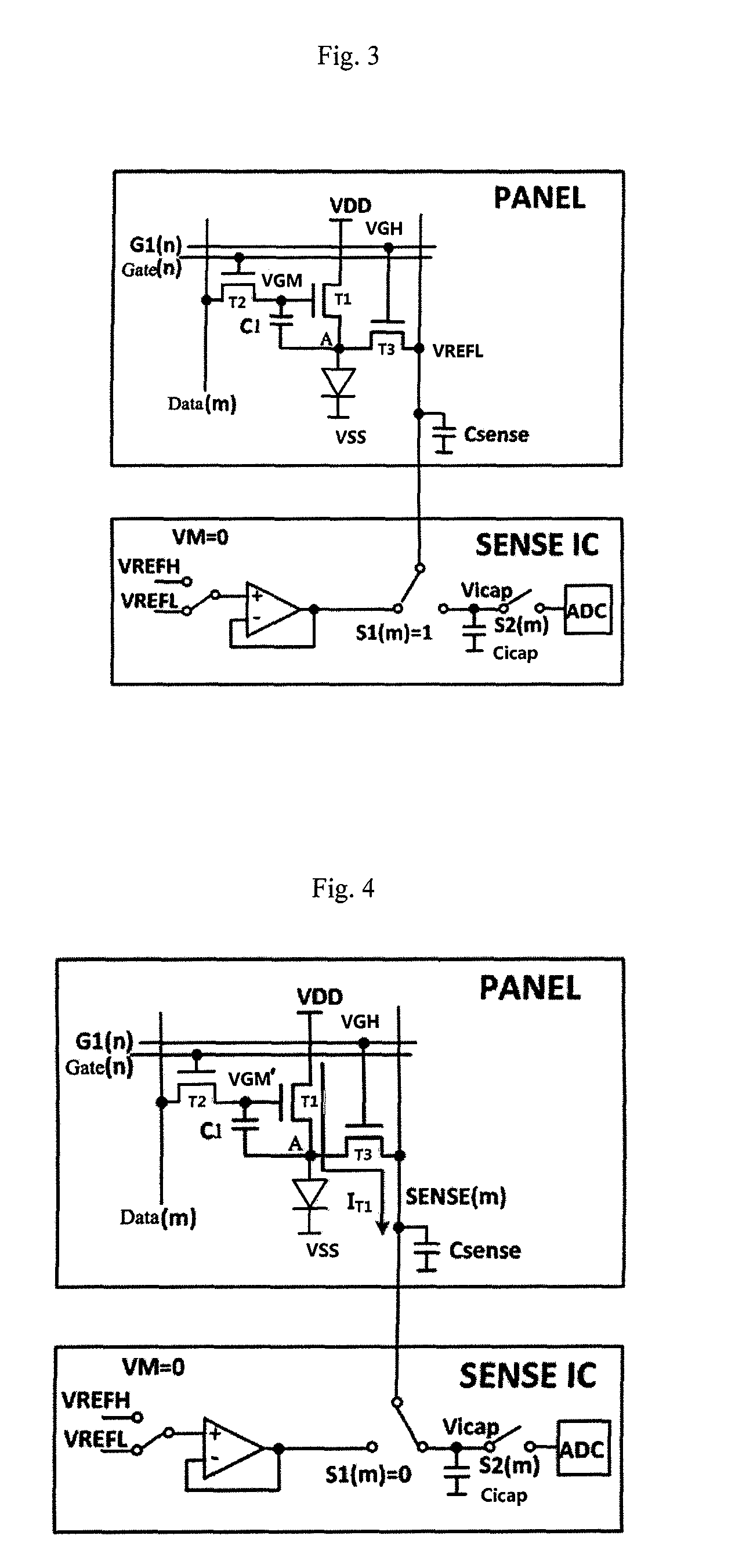
[0029]FIG. 1 shows an OLED driving compensation circuit provided by an embodiment of the present invention. In this embodiment, the OLED driving compensation circuit includes a driving module 1 and an external compensation module 2. The driving module 1 includes a driving transistor T1 and a storage capacitor C1; a first electrode of the driving transistor T1 is connected with a power supply voltage terminal VDD, and a second electrode of the driving transistor T1 is connected with an OLED; a first terminal of the storage capacitor C1 is connected with the control electrode of the driving transistor T1, and a second terminal of the storage capacitor C1 is connected b...


PUM


Abstract

An OLED driving compensation circuit and a driving method thereof are provided. The circuit comprises an external compensation module and a driving module comprising a driving transistor and a storage capacitor. The driving transistor is respectively connected with a power supply voltage terminal and an OLED via a first electrode and a second electrode thereof, a first terminal of the storage capacitor is connected with a control electrode of the driving transistor, and a second terminal thereof is connected between the driving transistor and the OLED. The external compensation module is connected between the driving transistor and the OLED and provides a reference voltage to the electrode of the driving transistor connected with the second terminal of the storage capacitor, to reset the voltage on the electrode. The power supply voltage terminal as variable voltage source inputs a first voltage equal to the reference voltage when the voltage is reset.

Description

FIELD OF THE INVENTION[0001]The present invention relates to the field of display technology, and specifically relates to an OLED driving compensation circuit and a driving method thereof.BACKGROUND OF THE INVENTION[0002]In an AMOLED display device, the luminescence brightness of each OLED is determined by driving current generated by a driving circuit, and the driving current generated by the driving circuit can be expressed by the following formula:IOLED=K·(Vgs−Vth)2,[0003]wherein K is a parameter related with the process parameter and the feature size of a driving transistor, Vgs is the voltage difference between the gate and the source or between the gate and the drain of the driving transistor (determined by the type of the driving transistor), and Vth is the threshold voltage of the driving transistor.[0004]When the AMOLED display device displays a frame of picture, the threshold voltage Vth of the driving transistor may drift, and the driving current IOLED is changed, so that...

Claims


Application Information

Patent Timeline
Patent Type & Authority Patents(United States)
IPC IPC(8): H05B33/08H05B44/00G09G3/3225
CPCH05B33/0896G09G3/3233G09G2310/066G09G2320/0223G09G2320/0295H05B45/60Y02B20/30
Inventor GAI, CUILISONG, DANNAZENG, QINGHUI
Owner BOE TECH GRP CO LTD
Learn More