OLED pixel blending compensation circuit and blending compensation method

A pixel mixing and compensation circuit technology, applied to instruments, static indicators, etc., can solve problems such as inability to guarantee consistent luminous brightness, limited range of compensation, and complicated compensation process

Active Publication Date: 2017-03-15
SHENZHEN CHINA STAR OPTOELECTRONICS TECH CO LTD
View PDF4 Cites 62 Cited by
  • Summary
  • Abstract
  • Description
  • Claims
  • Application Information

AI Technical Summary

Problems solved by technology

The method of achieving threshold voltage compensation simply by adding new thin film transistors and signal lines inside the pixel is called internal compensation. The compensation process is relatively simple and the operation speed is fast, but the pixel circuit is complicated and the range of compensation is limited; The method of performing threshold voltage compensation through an external integrated circuit (IC) chip on the panel is called external compensation. The pixel circuit is relatively simple and the compensation range is relatively large, but the compensation process is complicated and the operation speed is slow.
[0007] In addition, due to the aging and decline of organic light-emitting diodes, not only the threshold voltage rises, but even when the same current flows, the luminance of organic light-emitting diodes before and after the decline will also decrease. Internal compensation can only compensate the threshold voltage at most to ensure current flow The current through the organic light-emitting diodes is the same, and the brightness of the light cannot be guaranteed to be consistent

Method used


Image

  • OLED pixel blending compensation circuit and blending compensation method
  • OLED pixel blending compensation circuit and blending compensation method
  • OLED pixel blending compensation circuit and blending compensation method

Examples


Embodiment Construction

[0081] In order to further illustrate the technical means and effects adopted by the present invention, the following describes in detail in conjunction with preferred embodiments of the present invention and accompanying drawings.

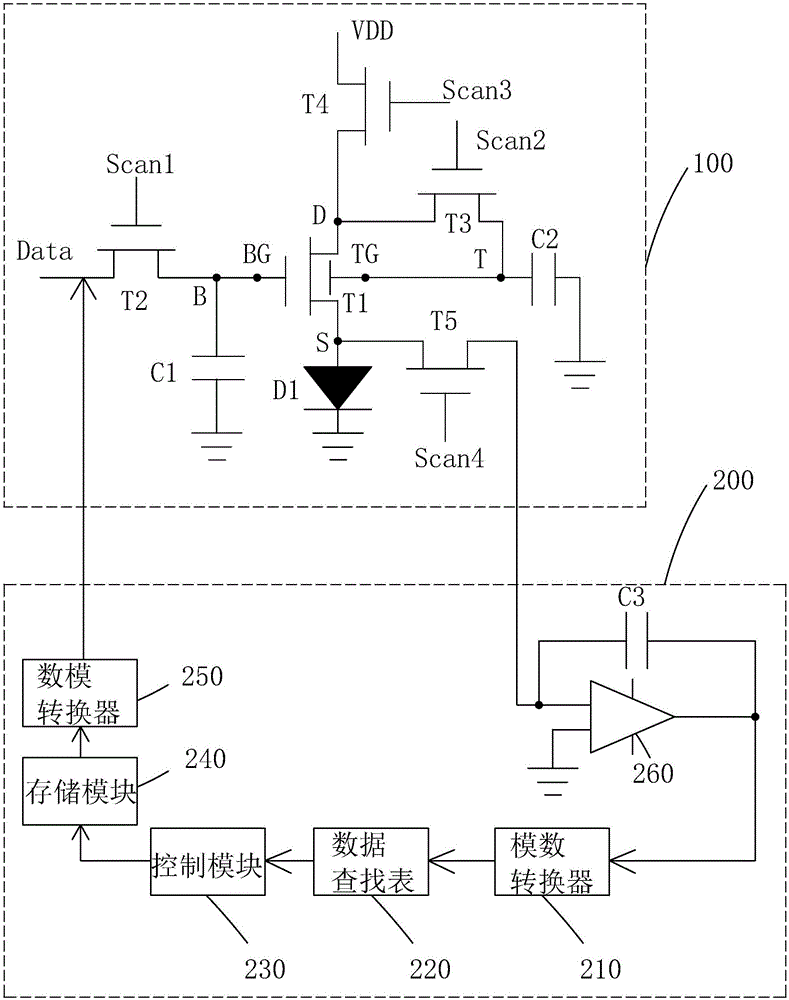
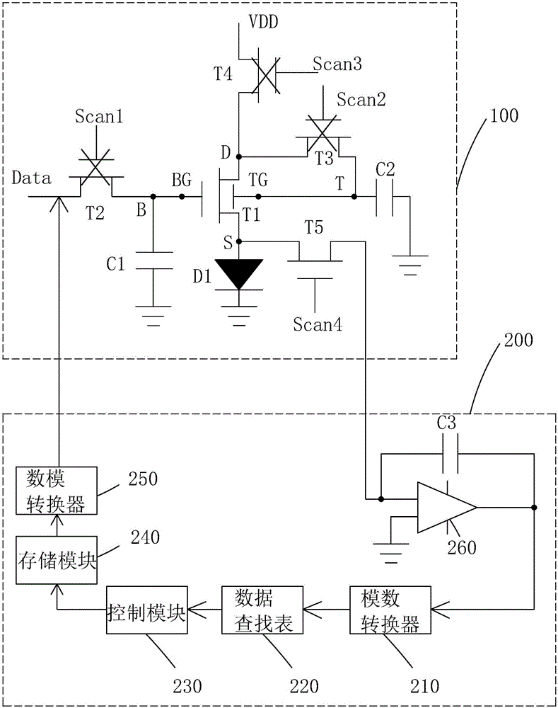
[0082] see figure 1 and figure 2 Firstly, the present invention provides an OLED pixel mixing compensation circuit, including a pixel internal driving circuit 100 and an external compensation circuit 200 electrically connected to the pixel internal driving circuit 100 .

[0083] The pixel internal driving circuit 100 includes: a first thin film transistor T1, a second thin film transistor T2, a third thin film transistor T3, a fourth thin film transistor T4, a fifth thin film transistor T5, a first capacitor C1, a second capacitor C2, and Organic Light Emitting Diode D1.

[0084] The first thin film transistor T1 is a double gate thin film transistor, its top gate TG is electrically connected to the first node T, its bottom gate BG is electrica...


PUM


Abstract

The present invention provides an OLED pixel blending compensation circuit and a blending compensation method. A 5T2C structure is employed and a thin film transistor is driven to compensate the threshold-voltage drift for a pixel internal drive circuit (10) of a bigrid thin film transistor, and an external compensation circuit (200) is employed to compensate the non-uniform brightness of an organic light-emitting diode (D1) caused by aging and declination. Through combination of the rapid internal compensation operation speed and the big external compensation range, the OLED pixel blending compensation circuit and the blending compensation method have better compensation effects, simplify the data signals (Data) and realize the uniform brightness of the panel through the stability of the OLED current.

Description

technical field [0001] The invention relates to the field of display technology, in particular to an OLED pixel mixing compensation circuit and a mixing compensation method. Background technique [0002] Organic light emitting diode (Organic Light Emitting Display, OLED) display device has self-illumination, low driving voltage, high luminous efficiency, short response time, high definition and contrast, nearly 180° viewing angle, wide operating temperature range, and can realize flexible display and With many advantages such as large-area full-color display, it is recognized by the industry as a display device with the most potential for development. [0003] OLED display devices can be divided into passive matrix OLED (Passive Matrix OLED, PMOLED) and active matrix OLED (Active Matrix OLED, AMOLED) two categories according to the driving method, namely direct addressing and thin film transistor (Thin Film Transistor, TFT) matrix addressing two types. Among them, AMOLED h...

Claims


Application Information

Patent Timeline
Patent Type & Authority Applications(China)
IPC IPC(8): G09G3/3233G09G3/3225
CPCG09G3/3225G09G3/3233G09G2320/046
Inventor 聂诚磊
Owner SHENZHEN CHINA STAR OPTOELECTRONICS TECH CO LTD
Why Eureka
Try Eureka