Flexible video displays and their manufacture

a flexible, video display technology, applied in the direction of static indicating devices, non-linear optics, instruments, etc., can solve the problems of lack of picture quality, lack of resource-hungry cathode ray tubes, and limited application prospects, so as to achieve simple manufacturing processes, excellent performance characteristics, and high yield

Active Publication Date: 2010-04-27
NEW VISUAL MEDIA GROUP
View PDF18 Cites 57 Cited by
  • Summary
  • Abstract
  • Description
  • Claims
  • Application Information

AI Technical Summary

Benefits of technology

[0172]An advantage of the invention is that flaps 30 do not have to be individually actuated, requiring independent and separate application of a voltage across the shutter between its fixed and movable electrodes, and requiring the complexity of a multiplexed drive signal, with the difficult timing constraints of needing a separate pulse for every shutter in the frame within the refresh interval. For this purpose, the shutters can be individually actuated by employing half-select drive circuitry wherein the fixed electrodes are electrically interconnected in rows and the movable electrodes, (e.g. metallized flaps or shutters) are interconnected in columns, or vice versa. By delegating addressability of the pixels within the column to the LED assemblies 16, pursuant to the present invention, the addressing and switching requirements of shutter array 12 can be simplified, so that flaps 30 of each row R1-RN can be switched in unison. The conductor configuration needed for row-by-row switching is relatively simple.
[0173]The fixed electrode can be, and preferably is, a common ground plane extending substantially uniformly across every pixel, for example conductive, ITO layer 36. Flaps 30 are then electrically interconnected in rows. Such interconnection can be achieved by employing a conductive material for the lines of adhesive 42, or via metallization of outer surface 32. The metallization of outer surface 32 should have bands of separation between the rows to isolate the rows electrically which banding can be achieved either by initially applying aluminum to PET film in bands, or more preferably, since metallized PET film is commercially available, by subsequently removing strips of metallization between the rows, for example by laser etching. Row terminations 44 (FIG. 1) can be used to bring current individually to each row R1-RN.Control Circuitry
[0174]Electronic control circuitry connected to the display, and described in more detail below in connection with FIG. 12, comprises an LED drive module and a shutter drive module. Operation of the LEDs is synchronized with shutter opening, by the drive circuitry. A data signal, for example a computer video signal, television picture signal, video text signal, video game signal, display advertising signal, or the like, is input to the control circuitry and is interpreted by the control circuitry to provide suitable drive signals for the hardware that will create the intended visual display when applied to LED assemblies 16 and shutters 14.
[0175]The light output of the LEDs can be controlled in two ways, by the amplitude of the current through the LED, and by the pulse width. Preferably, two intensity controls are provided, one control corresponding to the intensity of the video signal, and the other to compensate for light intensity losses as the output beam travels along light channels 20. The latter control is varied according to the vertical position of the shutter row being illuminated, greater compensation being provided for the topmost row, furthest from the LEDs.
[0176]Optionally, the drive current amplitude can be reduced as the image is scanned from the top to the bottom of the display, while the brightness of each pixel, as called for by the image data, is determined independently by the pulse width. As the scan approaches the line of LED assemblies 16, across the bottom of the display, the current, and therefore the power into the display is reduced.Operation
[0177]In operation, a biasing voltage is applied to all the shutters 14 in shutter array 12, to hold shutter elements 30 closed against polypropylene dielectric layer 38. Each shutter 14 blocks off a portion of its underlying light channel 20, preventing light from the respective LED assembly 16 associated with the light channel 20 from emerging through that particular pixel to the viewer. This is the default shutter position, in which the pixel appearance is that of outer surface 32 of shutter element 30, a reflective appearance in preferred embodiments. With all shutters 14 closed, display panel 10 has a continuous mirror-like appearance, reflecting ambient light.

Problems solved by technology

And few businessmen, scientists or teachers can properly practice their professions without the ubiquitous personal computer and its accompanying display.
Surprisingly, prior to this invention, the display device is, all too often, a bulky, heavy, resource-hungry, energy-consuming cathode ray tube.
Though alternative technologies proliferate, they either lack picture quality or are more expensive, limiting their fields of use.
A drawback of conventional displays known to the present inventors is that they have a fixed form, typically comprising a rigid rectangular display panel which provides the viewed display area.
A drawback of such displays is their reliance upon side-by-side RGB subpixels to achieve full color which limits the light output.
The display intensity, or luminance of displayed primary colored images is limited by the need for an individual subpixel to illuminate the area of the group of three (or possibly four) subpixels, and manufacturing is complicated.
Such synthesis of electronically controllable optically active elements requires expensive techniques such as sputtering, vapor deposition, etching, and the like, may require exotic or exceptionally pure materials and the fabricated elements may be subject to contamination by ordinary structural materials such as common plastics materials that it would be desirable to use for substrates.
In addition to the expense and manufacturing difficulties, the materials needed for synthesis of active devices, and the restraints on the substrate materials that can be used, may effectively impose requirements of rigidity on the end product display panel.
Furthermore, such known flat panel display technologies require x-y addressing of individual pixels employing extended conductor patterns and raising multiplexing issues resulting from the electrical cross-coupling of the rows and columns in the display medium.
In addition to their cost, such measures may limit luminance, contrast or gray scale quality or the ability to refresh the display at video rates.
Such leakage is the cause of cross talk.
Cross-coupling in a display with an indistinct threshold can cause a display to partially illuminate when or where it is not intended to illuminate.
However, active matrix displays are relatively expensive.
In addition, active matrix technologies, used in organic light-emitting diode (“OLED”) displays, and some liquid crystal displays (“LCD”), have other drawbacks.
For example, fabrication of an active matrix display on a flexible substrate can be particularly difficult.
Barrier layers needed for active matrices, even on glass, complicate manufacture and have been shown to delay damage rather than provide complete protection.
Such processes typically require the substrate to be heated, creating difficulties with plastic substrates which may change their dimensions, deleteriously affecting the alignment of components in subsequent masking steps.
In the case of passive technologies for LCD, OLED or other displays the fabrication of long, narrow row or column electrodes from transparent conductive materials for example indium tin oxide (“ITO” herein), with sufficient current carrying capability for operation of a matrix display can be expected to present significant technical difficulties because of the limited conductivity of the transparent materials.
Unavoidably high resistances in long conductors may cause line access times to be unduly high and cause excessive power consumption and heat generation.
Nor are passive matrix supertwist LCDs well suited to fabrication on or assembly with flexible plastic substrates because they require small and well controlled cell gap spacings.
Other liquid crystal technologies, including ferroelectric, cholesteric and bistable nematic devices, being passive displays, require currents at video rates and power levels that are difficult to supply on flexible substrates with known transparent conductors.
Difficulties are expected in attempting to use phosphors, such as are employed in laser-based polymer flat panel displays and OLEDs, on a flexible plastic substrate, because phosphors require a protected environment to prevent degradation.
These protected phosphor devices can have long lifetimes, whereas unprotected phosphors have rather short lives.
However, the light output of such electropolymeric displays is limited by the side-by-side subpixel configuration and a further drawback is the need for x-y addressing, or multiplexing of the shutter array.

Method used


Image

  • Flexible video displays and their manufacture
  • Flexible video displays and their manufacture
  • Flexible video displays and their manufacture

Examples


example 1

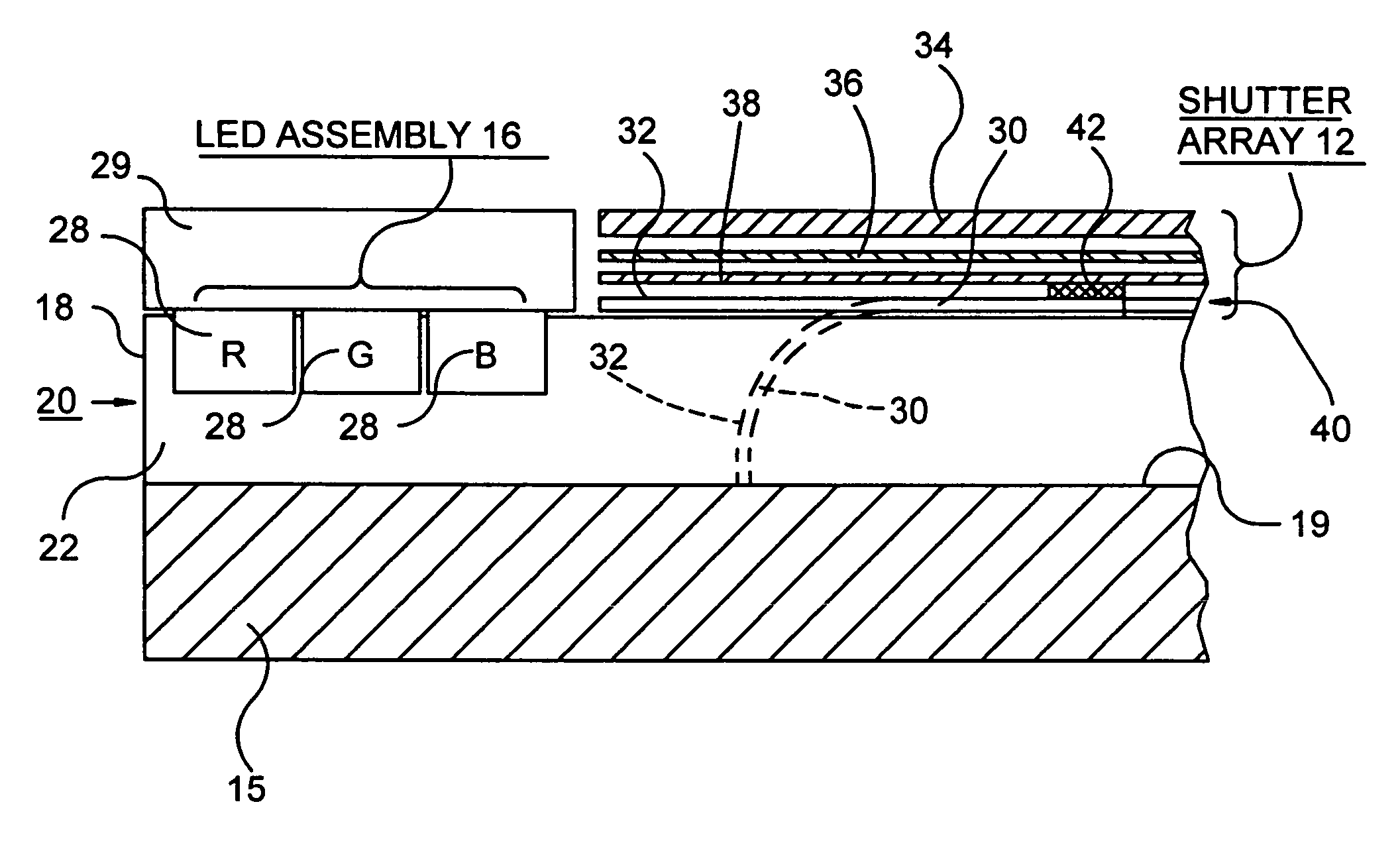
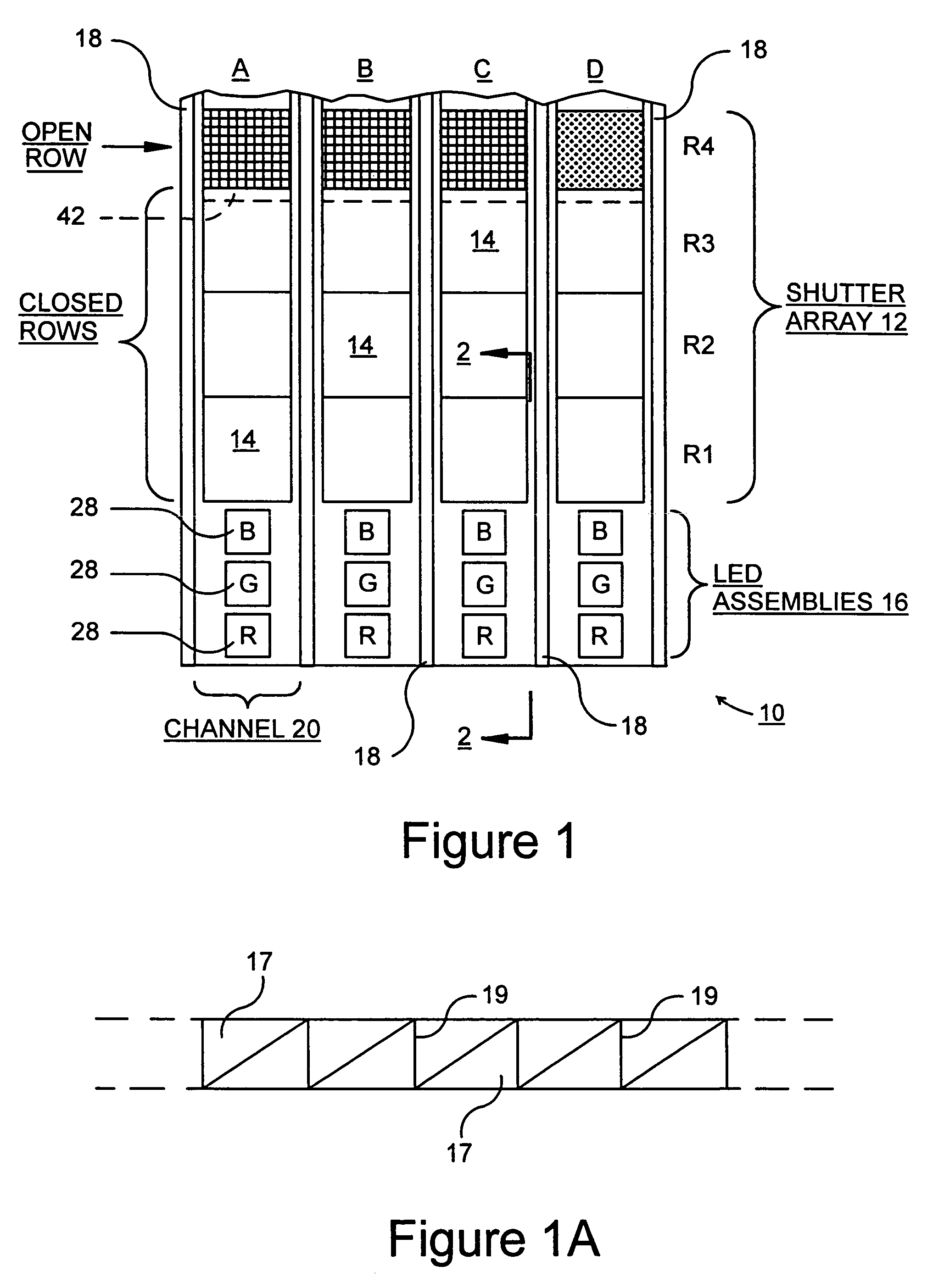
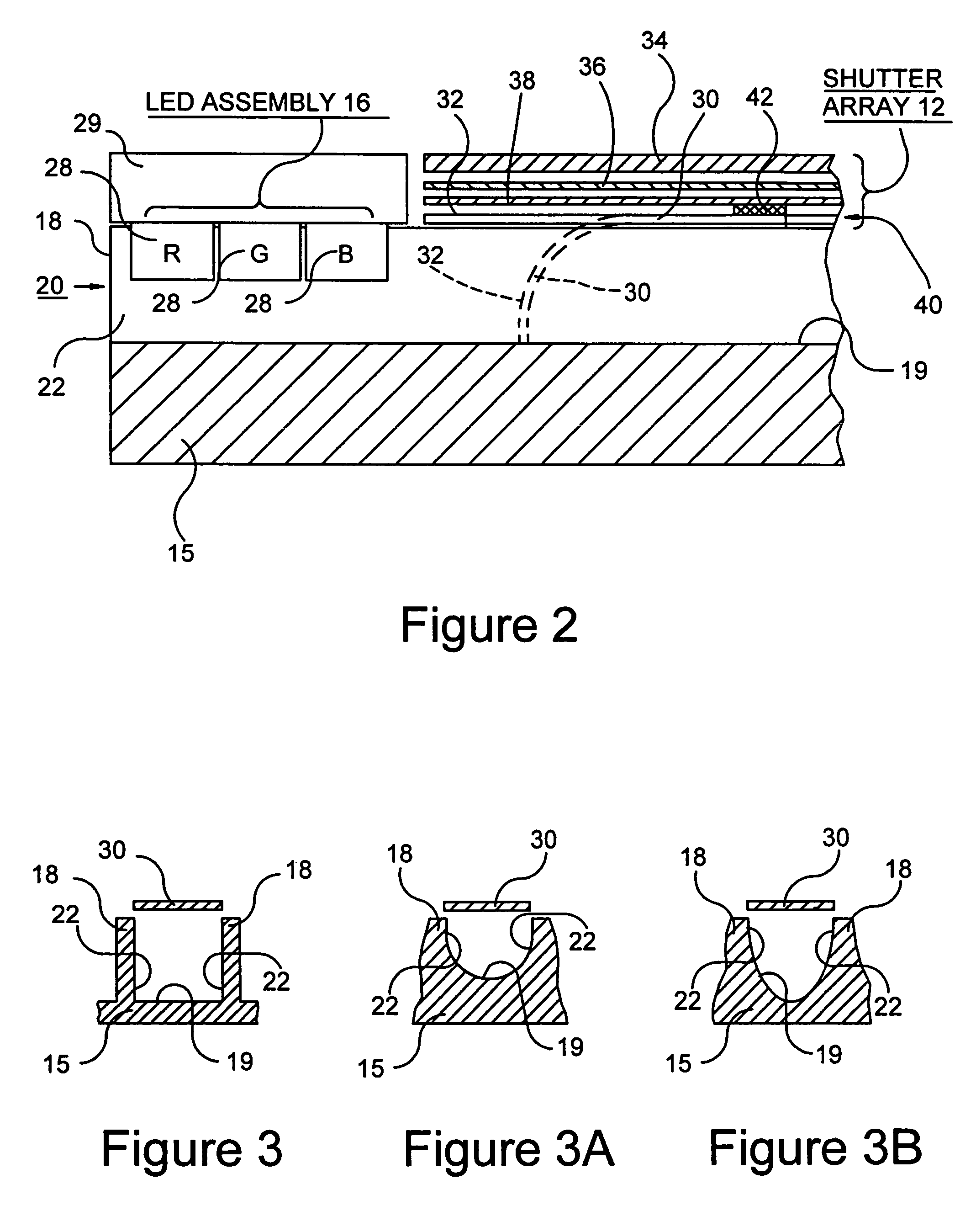
[0239]An exemplary full-color 15-inch VGA display (480 lines by 640 lines, about 53 lines per inch), according to the invention has a diagonal measurement of about 38 cm. (about 15 in.), a height of about 23 cm (about 9 in.) and a width of about 30 cm. (about 12 in.), implying a pixel size of about 0.45 mm (18 mil). The display is constructed as described above, with a shutter array 12 mounted on a channelized substrate or channel plate 15 and a line of LED assemblies 16 illuminating the light channels 20. The shutter array 12 comprises a common ITO fixed electrode film 36, a polypropylene dielectric film layer 38, and an orthogonal grid of rectangular shutter elements 30 cut from a metallized PEN film layer 40.

[0240]The LED assemblies comprise commercially available LED die, having an emitting area of about 0.25×0.25 mm (about 10 mil×10 mil), are employed emitting along each channel, giving an emitting area to pixel area ratio of about 1:3.24. Each LED assembly 16 comprises a combi...

example 2

[0247]Custom produced LED die are used to provide a display panel having 80 lines / inch, for a panel scaled to 50″ diagonal.

[0248]Referring now to FIG. 13, the illustrated method of displaying a pixellated video image can be effected, by way of example, by employing a video display panel device or apparatus such as that described herein, or other such display devices or apparatus, as will be apparent to those skilled in the art.

[0249]The display method comprises projecting a number of optically modulatable light beams from an array of light sources in side-by-side parallel bands across the display area. The light beams are pulsed in accordance with a timing signal and the character of light in each pulse, e.g. with respect to chrominance and luminance, is preferably determined by a drive signal. The light sources can comprise groups of three primary colored sources addressing each band, for example LED assemblies 16, or other suitable light sources capable of being modulated to provi...


PUM


Abstract

A flat panel display has a linear array of switchable light emitting diodes (“LEDs”) to emit bands of light across the display, providing a light pattern programmable at video frequencies and a two-dimensional electropolymeric shutter array to convert the light pattern into a video image. The light pattern can be varied or controlled spatially, with respect to both hue and intensity, by suitable drive signals, at points along the array determined by the location of individual LEDs, or groups of LEDs, and temporally as the shutters in the array are opened and closed to provide a pleasing full color gamut for every pixel in the display. Closed shutters, displaying a reflective appearance, can be employed for background or other effects. The shutter array can be flexibly constructed and supported on a flexible substrate to provide a flexible display.

Description

BACKGROUND OF THE INVENTION[0001]1. Field of the Invention[0002]This invention relates to electronically driven video displays for displaying computer, television or other informational or entertainment images or text which displays can have flexible shape enabling novel displays according to the invention to be curved, rolled, flexed or folded. The inventive displays can be embodied in a wide variety of forms, including high definition television monitors, laptop and desktop computer monitors, cell phone displays, sports stadium displays, highway signs and the like, in conventional configurations, and also in novel, variable form configurations. The invention also relates to the manufacture of such displays.[0003]2. Description of Related Art[0004]Including Information Disclosed under 37 CFR 1.97 and 37 CFR 1.98[0005]In the emerging information age, at the beginning of the twenty-first century, video display panels are commonplace household and office items appearing in many forms....

Claims


Application Information

Patent Timeline
Patent Type & Authority Patents(United States)
IPC IPC(8): G09G3/34
CPCG09G3/34G09G3/342G09G3/3413G09G3/346G09G2320/0666G09G2320/0633G09G2320/064G09G2320/0646G09G2310/024
Inventor KALT, CHARLES G.KALT, THOMAS F.MILLER, ROBERTSEELEY, WILLIAM G.SLATER, MARK S.
Owner NEW VISUAL MEDIA GROUP
Why Eureka
Try Eureka