Supercharge Your Innovation With Domain-Expert AI Agents!

Method for performing deep n-typed well-correlated (DNW-correlated) antenna rule check of integrated circuit and semiconductor structure complying with DNW-correlated antenna rule

a technology of well-correlated and integrated circuits, applied in semiconductor/solid-state device testing/measurement, semiconductor/solid-state device details, instruments, etc., can solve problems such as device failure, region, fragile and highly susceptible to damage, and achieve the effect of preventing and facilitating detection

Active Publication Date: 2017-03-28
UNITED MICROELECTRONICS CORP
View PDF36 Cites 2 Cited by
  • Summary
  • Abstract
  • Description
  • Claims
  • Application Information

AI Technical Summary

Benefits of technology

[0010]According to the present invention, a semiconductor monitoring device is provided. By landing the die seal ring on a large-area DNW, the DNW-correlated antenna effect is amplified and thus is easily detected by the monitoring device, which is electrically connected to the die seal ring. According to the present invention, a method for performing a DNW-correlated antenna rule check of an integrated circuit is provided. The method includes an inequality that must be complied. When the inequality is violated, the design layout of the integrated circuit must be adjusted, corrected, and / or re-designed. That is, the method for performing the DNW-correlated antenna rule check of the integrated circuit of the present invention provides a practical inequality to guide the layout designer so that the DNW-correlated antenna effect can be efficaciously prevented. Accordingly, a semiconductor structure formed in accordance with the design layout is obtained, and the semiconductor device is protected from the DNW-correlated antenna effect.

Problems solved by technology

It therefore results another issue due to the thinner gate dielectric layer: The thinner gate dielectric layer, which overlies the channel region, is fragile and highly susceptible to damages from external sources during manufacturing processes.
Should any damages caused to the gate dielectric layer, gate leakage current is inevitably increased, and it even causes device failure.
Consequently, it is concluded that such damage is getting worse when the DNW area ratio is increased.

Method used


Image

  • Method for performing deep n-typed well-correlated (DNW-correlated) antenna rule check of integrated circuit and semiconductor structure complying with DNW-correlated antenna rule
  • Method for performing deep n-typed well-correlated (DNW-correlated) antenna rule check of integrated circuit and semiconductor structure complying with DNW-correlated antenna rule
  • Method for performing deep n-typed well-correlated (DNW-correlated) antenna rule check of integrated circuit and semiconductor structure complying with DNW-correlated antenna rule

Examples


Embodiment Construction

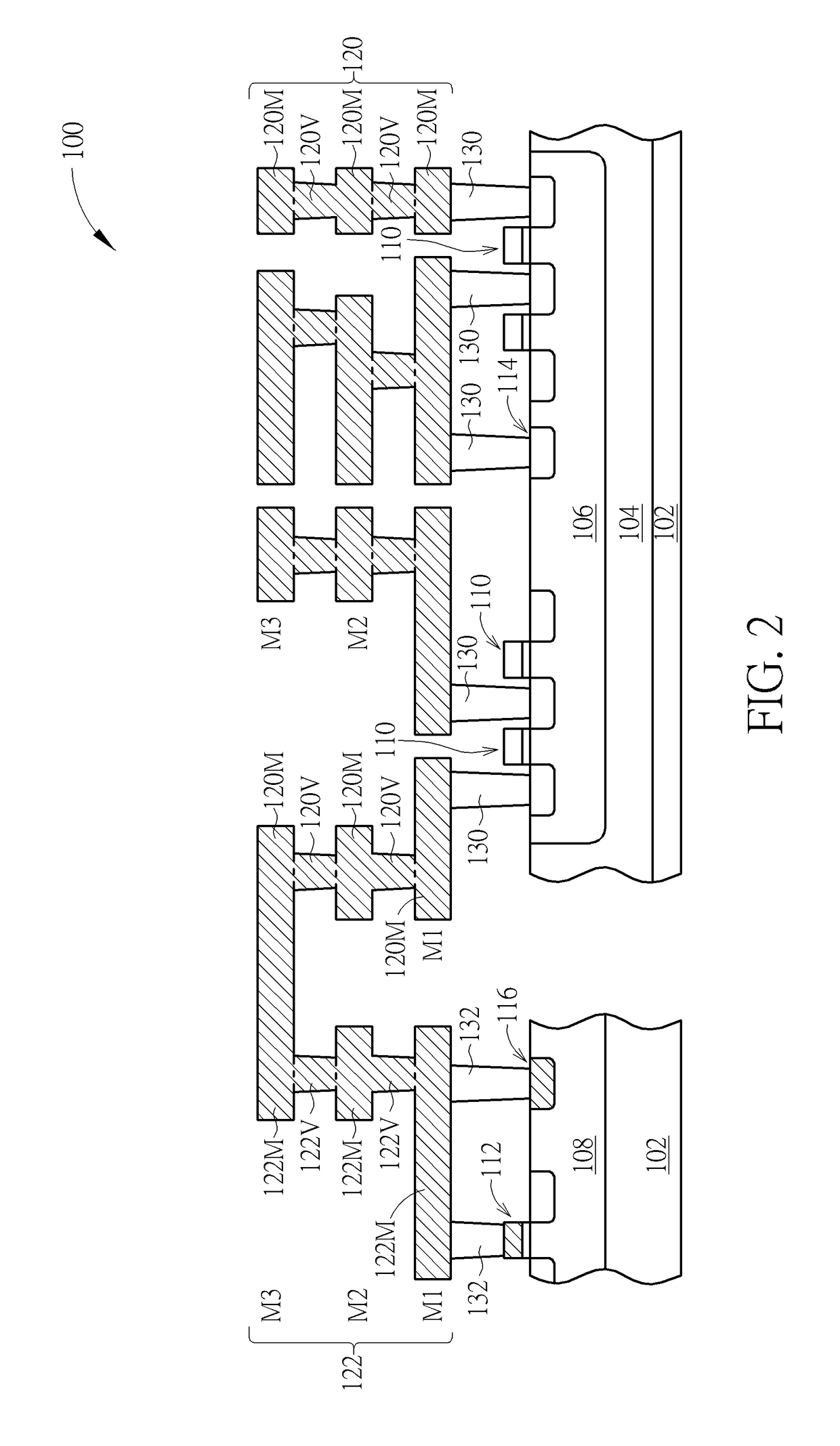
[0020]Please refer to FIG. 2, which is a schematic drawing illustrating a semiconductor structure. The semiconductor structure 100 includes a p-typed substrate (hereinafter abbreviated as p-substrate) 102, and a first p-typed well 106 and a second p-typed well 108 are formed in the p-substrate 102. The first p-typed well 106 and the second p-typed well 108 are physically spaced apart from each other. It is noteworthy that a deep n-typed well (DNW) 104 is formed in the p-substrate 102 in order to prevent noise, and the first p-typed well 106 is formed in and encompassed by the DNW 104. A plurality of first devices 110 are formed in the first p-typed well 106 in the DNW 102 and at least a second device 112 is formed in the second p-typed well 108 in the p-substrate 102. The first devices 110 and the second device 112 respectively can be a metal-oxide-semiconductor field effect transistor (hereinafter abbreviated as MOSFET) device, and the MOSFET device includes a gate electrode, a sou...


PUM


Abstract

A semiconductor monitoring device includes a substrate, a die seal ring formed on the substrate, a deep n-typed well formed in the substrate under the die seal ring, and a monitoring device electrically connected to the die seal ring. The monitoring device is formed in a scribe line region defined on the substrate. A width of the deep n-typed well is larger than a width of the die seal ring.

Description

BACKGROUND OF THE INVENTION[0001]1. Field of the Invention[0002]The invention relates to a monitoring semiconductor device, a method for performing a deep n-typed well-correlated (hereinafter abbreviated as DNW-correlated) antenna rule check of an integrated circuit, and a semiconductor structure complying with the DNW-correlated antenna rule.[0003]2. Description of the Prior Art[0004]With rapid advancement of semiconductor fabricating technology, the integration level of integrated circuits (ICs) is bound to increase continuously in order to improve the device speed and performance. And the continuing shrinkage of the device dimensions, which in order to comply with current requirements for light weight, slimness, and compactness, involves a plurality of issues associated therewith, such as a thinner gate dielectric layer is required.[0005]It therefore results another issue due to the thinner gate dielectric layer: The thinner gate dielectric layer, which overlies the channel regio...

Claims


Application Information

Patent Timeline
Patent Type & Authority Patents(United States)
IPC IPC(8): G06F17/50H01L21/66H01L23/58H01L27/06H01L23/10H01L27/02H01L21/8238H01L23/00H01L23/528
CPCG06F17/5081H01L22/34H01L23/58H01L21/823871H01L23/10H01L23/528H01L23/562H01L27/0266H01L27/0629H01L2924/0002H01L2924/00G06F30/398
Inventor ZHANG, XING HUAKU, CHI-FALIAO, HONGLI, YE CHAOYANG, HUI
Owner UNITED MICROELECTRONICS CORP
Features
  • R&D
  • Intellectual Property
  • Life Sciences
  • Materials
  • Tech Scout
  • Unparalleled Data Quality
  • Higher Quality Content
  • 60% Fewer Hallucinations
Learn More