
Imaging module and electronic device

a technology of imaging module and electronic device, which is applied in the direction of printers, instruments, cameras focusing arrangements, etc., can solve the problems of increasing the manufacturing cost of imaging modules and high cost of imaging modules, and achieve the effect of low cost and high accuracy

Active Publication Date: 2017-03-28
NANCHANG O FILM OPTICAL ELECTRONICS TECH CO LTD
View PDF8 Cites 5 Cited by
  • Summary
  • Abstract
  • Description
  • Claims
  • Application Information

AI Technical Summary

Benefits of technology

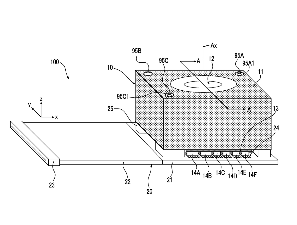
[0013]By performing positioning of the lens unit and the imaging element unit in a state where the position of the lens moved by gravity is held at a predetermined position, it is possible to accurately perform the positioning.
[0015]According to a decrease in a size of the lens unit, since a size of the terminal also decreases, it is necessary to perform positioning of the terminal and the probe pin with high accuracy. However, in order to position the terminal and the probe pin with high accuracy, high cost in a manufacturing apparatus of the imaging module, or complication in a manufacturing method of the imaging module occurs, and a manufacturing cost of the imaging module increases.
[0016]The present invention is made in consideration of the above-described circumstances, and an object thereof is to provide an imaging module capable of performing positioning of the imaging element unit and the lens unit at a low cost and with high accuracy, and an electronic device having the imaging module.
[0019]According to the present invention, it is possible to provide an image module capable of performing positioning of the imaging element unit and the lens unit at a low cost and with high accuracy, and the electronic device having the imaging module.

Problems solved by technology

However, in order to position the terminal and the probe pin with high accuracy, high cost in a manufacturing apparatus of the imaging module, or complication in a manufacturing method of the imaging module occurs, and a manufacturing cost of the imaging module increases.

Method used


Image

  • Imaging module and electronic device
  • Imaging module and electronic device
  • Imaging module and electronic device

Examples


first modification example

[0114]FIG. 7 is an external perspective view of an imaging module 200 which is a modification example of the imaging module 100.

[0115]The imaging module 200 has the same configuration as the imaging module 100 except that the positions of the terminals 14A and 14B of the lens unit 10 are changed.

[0116]In the imaging module 100, in the arrangement direction (x direction) of the terminals 14A to 14F, other terminals do not exist between the terminal 14A and the terminal 14B having a large exposed area. Meanwhile, in the imaging module 200, other terminals to which electricity does not flow during the adjustment process exist between the terminal 14A and the terminal 14B and are arranged therebetween.

[0117]According to this arrangement, it is possible to increase the distance between the terminals which come into contact with the probe pins during the adjustment process. Accordingly, an electrical connection between the probe unit 113 and the terminals 14A and 14B is more easily perfor...

second modification example

[0118]FIG. 8 is an external perspective view of an imaging module 300 which is a modification example of the imaging module 100.

[0119]In the imaging module 100, the terminal 14A to the terminal 14F are arranged in the direction along one side of outer edges of the imaging element 27 in a plan view. Meanwhile, the imaging module 300 is different from the imaging module 100 in that the terminal 14A to the terminal 14F are arranged in directions along two sides different from each other (in the example of FIG. 8, the side parallel to the x direction and the side parallel to the y direction in a plan view) of the outer edges of the imaging element 27 in a plan view.

[0120]Moreover, in the imaging module 300, the dispositions of the terminals 24A to 24F provided on the substrate 21 are changed according to the changes of the dispositions of the terminal 14A to the terminal 14F.

[0121]Among the terminals included in the lens unit terminal portion of the imaging module 300, the terminals 14A...

third modification embodiment

[0123]In the manufacturing processes of the imaging module 100 and the imaging module 300, it is possible to perform the positioning having high accuracy by driving the first lens driving unit included in the lens unit 10. In order to increase the accuracy, the positioning may be performed in a state where electricity flows to the z-direction hall element 16B included in the lens drive unit 16.

[0124]That is, probes, which come into contact with the four terminals 14a to 14d connected to the z-direction hall element 16B, may be provided on the probe unit 113 of the manufacturing apparatus 30.

[0125]In addition, in the adjustment process, in a state where electricity flows to the terminals 14A and 14B and the terminals 14a to 14d and the position in the z direction of the lens group 12 is held with high accuracy using the signals detected by the z-direction hall element 16B, the control unit 85 may perform the imaging of the measurement chart 89.

[0126]In this way, it is possible to con...


PUM


Abstract

An imaging module 100 includes a lens unit 10 and an imaging element unit 20. The lens unit 10 includes a VCM 16A which moves a lens group 12 in a z direction, terminals 14A and 14B which are electrically connected to the VCM 16A, a VCM 16C and a VCM 16E which move the lens group 12 in an x direction and a y direction, and terminals 14C to 14F which are electrically connected to the VCM 16C and the VCM 16E. The imaging element unit 20 includes terminals 24A to 24F which are electrically connected to the terminals 14A to 14F. Exposed areas of the terminals 14A and 14B are larger than exposed areas of the terminals 14C to 14F.

Description

CROSS-REFERENCE TO RELATED APPLICATIONS[0001]This application is a Continuation of PCT International Application No. PCT / JP2014 / 068061 filed on Jul. 7, 2014, which claims priority under 35 U.S.C §119 (a) to Japanese Patent Application No. 2013-157721 filed on Jul. 30, 2013. Each of the above application(s) is hereby expressly incorporated by reference, in its entirety, into the present application.BACKGROUND OF THE INVENTION[0002]1. Field of the Invention[0003]The present invention relates to an imaging module and an electronic device having the imaging module.[0004]2. Description of the Related Art[0005]A small and thin imaging module is mounted on a portable electronic device such as a portable phone having a photographing function. The imaging module has a structure in which a lens unit in which a photographic lens is incorporated and an imaging element unit in which a Charge Coupled Device (CCD) image sensor, a Complementary Metal-Oxide Semiconductor (CMOS) image sensor, or the ...

Claims


Application Information

Patent Timeline
Patent Type & Authority Patents(United States)
IPC IPC(8): H04N5/232G02B7/08G03B5/00H04N5/225G03B3/10
CPCH04N5/2257G02B7/08G03B3/10G03B5/00H04N5/2253G03B2205/0069H04N23/54H04N23/57
Inventor YAMAKAWA, KENJIKANEKO, YUKIHIROTOBISE, MANABUFUJINAMI, TATSUYA
Owner NANCHANG O FILM OPTICAL ELECTRONICS TECH CO LTD
Learn More