Package, light emitting device, and methods of manufacturing the package and the light emitting device

a technology of light emitting devices and packaging, which is applied in the manufacturing of semiconductor/solid-state devices, semiconductor devices, electrical devices, etc., can solve the problems of resin burr generation and reduced led output, and achieve the effect of suppressing burr production, reducing the output of an led, and suppressing burr production

Active Publication Date: 2017-04-04
NICHIA CORP
View PDF15 Cites 0 Cited by
  • Summary
  • Abstract
  • Description
  • Claims
  • Application Information

AI Technical Summary

Benefits of technology

[0017]With the package and the light emitting device according to the embodiments of the present disclosure, production of burrs can be suppressed without reducing the output of an LED. Further, according to the methods of manufacturing a package and a light emitting device of the present disclosure, a package and a light emitting device in which production of burrs is suppressed without reducing the output of an LED can be manufactured.

Problems solved by technology

However, with such a method of manufacturing an LED, the resin flows into a gap between the lead frame and the mold, which may result in generation of resin burrs.
Such resin burrs may cause a bonding failure of LED elements and / or wires, so the burrs must be removed.
This contact results in formation of a mark in the LED mounting portion that reduces the glossiness of the plating, which may lead to a reduction in the output of the LED.

Method used


Image

  • Package, light emitting device, and methods of manufacturing the package and the light emitting device
  • Package, light emitting device, and methods of manufacturing the package and the light emitting device
  • Package, light emitting device, and methods of manufacturing the package and the light emitting device

Examples


embodiments

[0038]In the following, embodiments will be described with reference to the drawings. Each of the embodiments shown below exemplifies a light emitting device embodying the technical idea of the present invention;the technical idea of the present invention is not limited to the embodiments shown below. Further, the size, material, shape, relative arrangement and the like of constituent components described in the embodiments are not intended to limit the scope of the present invention thereto unless otherwise specified, and they are merely examples. Note that, the size, positional relationship and the like in the drawings may be exaggerated for the sake of clarity.

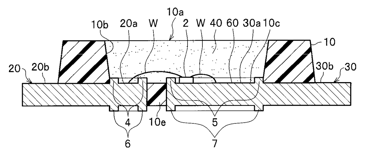
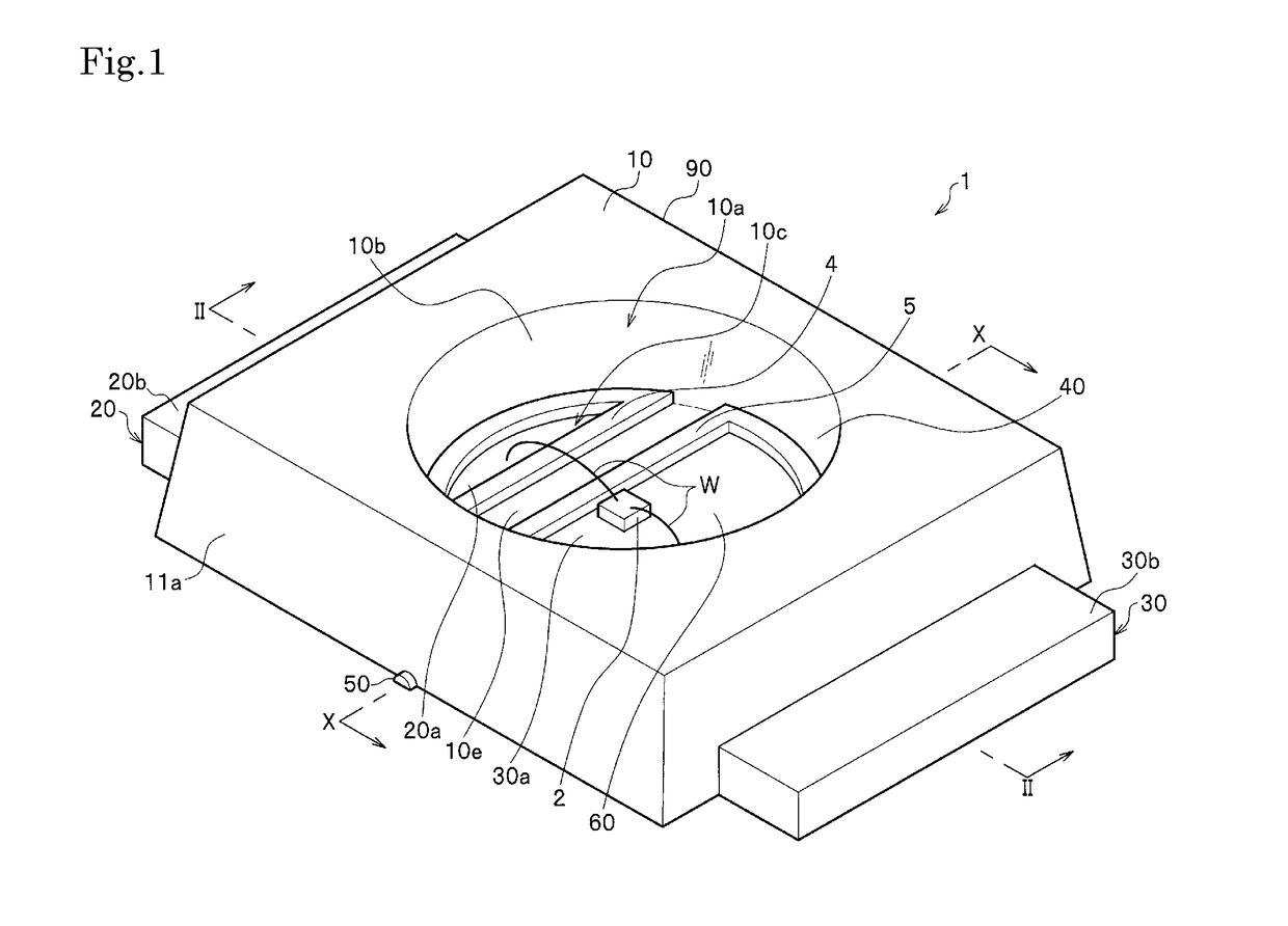
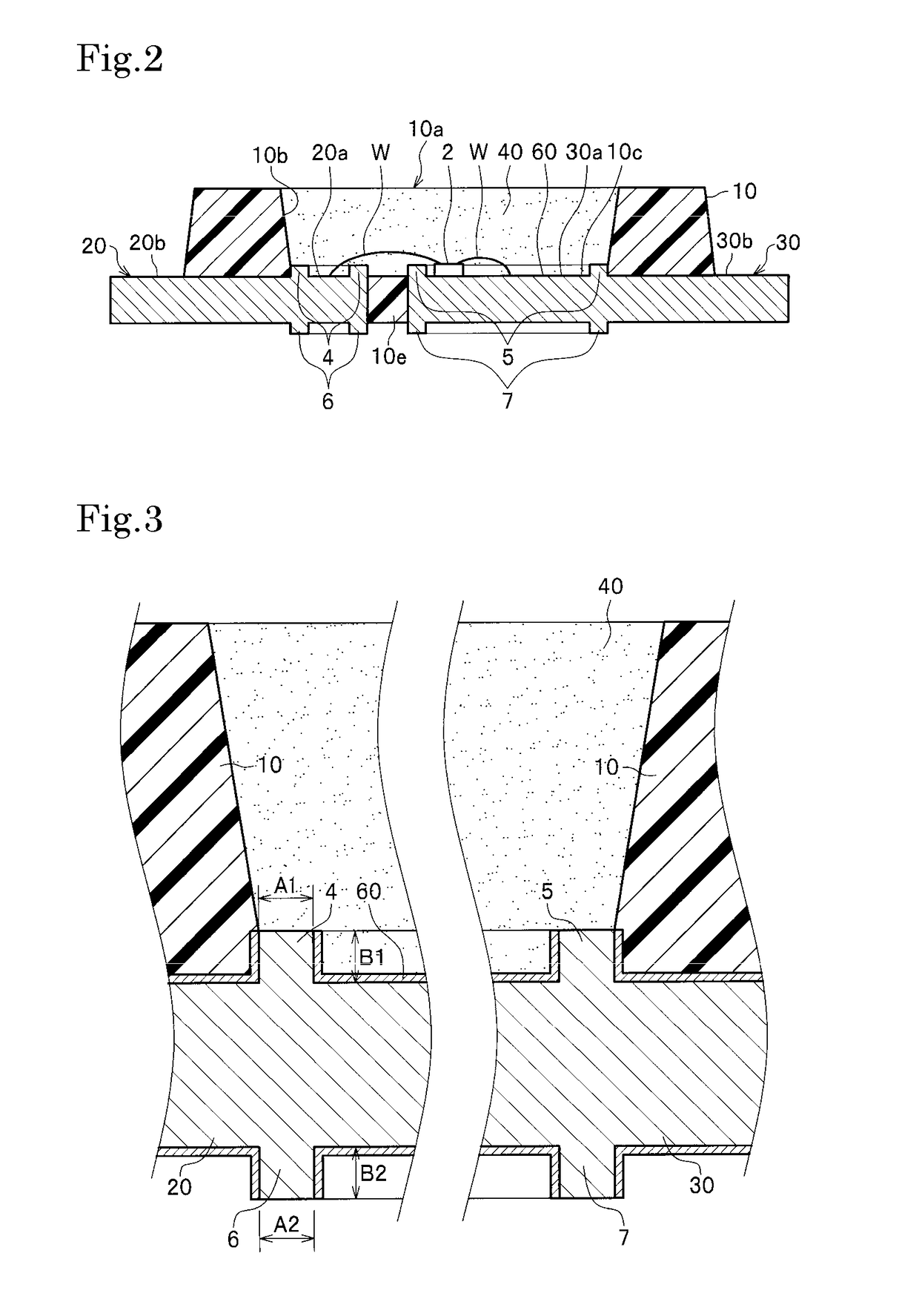
[0039]FIG. 1 is a schematic diagram of a cross section of a light emitting device according to one embodiment. FIG. 2 is a schematic diagram of a cross section of the light emitting device according to one embodiment taken along line II-II in FIG. 1. FIG. 3 is a partial schematic diagram of a cross-section of the light emit...

example 1

[0121]In the following, Example 1 of the present invention will be described. Molding was performed using, as shown in FIGS. 2 and 3, the first lead electrode 20 and the second lead electrode 30 provided with the front surface protrusions 4 and 5 at the boundary between the metal exposed portions of the first lead electrode 20 and the second lead electrode 30 and the resin molded body 10, and with the back surface protrusions 6 and 7 at the position on the back surface opposite to the position of the front surface protrusions 4 and 5, using a transfer molding machine.

[0122]The molding was performed under the conventional pressing pressure and injection pressure conditions with which resin burrs were produced when molding was performed using conventional lead electrodes without the front surface protrusions 4 and 5 and the back surface protrusions 6 and 7. Then, whether or not burrs were produced was checked.

[0123]As a result, it was found that burrs were not produced at the metal ex...


PUM


Abstract

A package for mounting a light emitting element includes a recess; a pair of lead electrodes exposed at a bottom surface of the recess; a plating layer covering a surface of each of the pair of lead electrodes; and a resin molded body retaining the pair of lead electrodes, and forming an area between the pair of lead electrodes at the bottom surface of the recess and a lateral surface of the recess. At least one of the lead electrodes has a front surface protrusion that is linearly formed along the resin molded body at the bottom surface of the recess and along a periphery of the bottom surface of the recess, and a back surface protrusion that is formed at a position at a back surface opposite to a position of the front surface protrusion, and at least a tip of each of the front surface protrusion and the back surface protrusion is exposed outside the plating layer.

Description

CROSS-REFERENCE TO RELATED APPLICATION[0001]This application claims priority to Japanese Patent Application No. 2014-263694 filed on Dec. 25, 2014. The entire disclosure of Japanese Patent Application No. 2014-263694 is hereby incorporated herein by reference.BACKGROUND[0002]1. Technical Field[0003]The present disclosure relates to a package, a light emitting device, and methods of manufacturing the package and the light emitting device.[0004]2. Description of the Related Art[0005]A method of manufacturing a light emitting diode (hereinafter referred to as an “LED”) includes molding a package, and an LED is manufactured through the molding step. In manufacturing an LED, transfer molding has been typically employed, in which a lead frame is set in a mold and liquid resin is injected. However, with such a method of manufacturing an LED, the resin flows into a gap between the lead frame and the mold, which may result in generation of resin burrs. Such resin burrs may cause a bonding fa...

Claims


Application Information

Patent Timeline
Patent Type & Authority Patents(United States)
IPC IPC(8): H01L33/00H01L33/62H01L33/48
CPCH01L33/62H01L33/486H01L2224/48091H01L2224/48247H01L2224/48257H01L2924/181H01L2933/0033H01L2933/0066H01L2924/00012H01L2924/00014H01L21/4846H01L21/565H01L33/52H01L2933/005
Inventor ABE, KOJISHIOTA, YUKI
Owner NICHIA CORP
Why Eureka
Try Eureka