Light emitting package and LED bulb

a technology of led bulbs and light emitting packages, which is applied in the direction of light sources, lighting device details, lighting and heating apparatuses, etc., can solve the problems of low heat dissipation efficiency of conventional led bulbs, low light emitting angle, and limited application of conventional leds, so as to reduce the arrangement density of led chips and achieve uniform light output

Active Publication Date: 2017-04-11
ADVANCED SEMICON ENG INC
View PDF35 Cites 0 Cited by
  • Summary
  • Abstract
  • Description
  • Claims
  • Application Information

AI Technical Summary

Benefits of technology

[0006]The arrangement density of the LED chips on the second surface of the first chip mounting portion near the second chip mounting portion is less than the arrangement density of the LED chips on the second surface of the first chip mounting portion away the second chip mounting portion. Similarly, the arrangement density of the LED chips on the second surface of the second chip mounting portion near the first chip mounting portion is less than the arrangement density of the LED chips on the second surface of the second chip mounting portion away the first chip mounting portion. By reducing the arrangement density of the LED chips near the junction of the first chip mounting portion and the second chip mounting portion, a uniform light output is achieved.

Problems solved by technology

However, the conventional LED bulb has the problem of low light emitting angle.
In addition, the plate substrate includes an insulation material therein, thus, the heat dissipating efficiency of the conventional LED bulb is low.
Therefore, the application of the conventional LED is limited.

Method used


Image

  • Light emitting package and LED bulb
  • Light emitting package and LED bulb
  • Light emitting package and LED bulb

Examples


Embodiment Construction

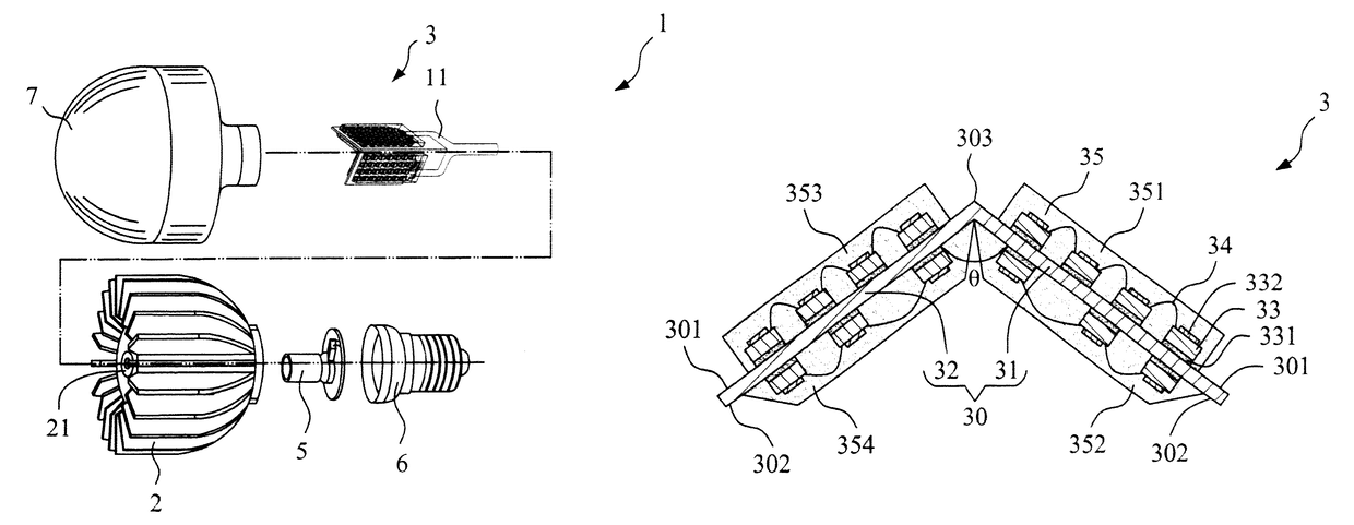
[0019]Referring to FIG. 1, a perspectively exploded view of a light emitting diode (LED) bulb 1 according to an embodiment is illustrated. The LED bulb 1 comprises a heat sink 2, a light emitting package 3, an optical housing 7, a power supply 5 and a socket 6. The heat sink 2 is used to dissipate the heat from the light emitting package 3. In this embodiment, the heat sink 2 has an opening 21 and a plurality of fins and the material of the heat sink 2 is copper (Cu) or aluminum (Al).

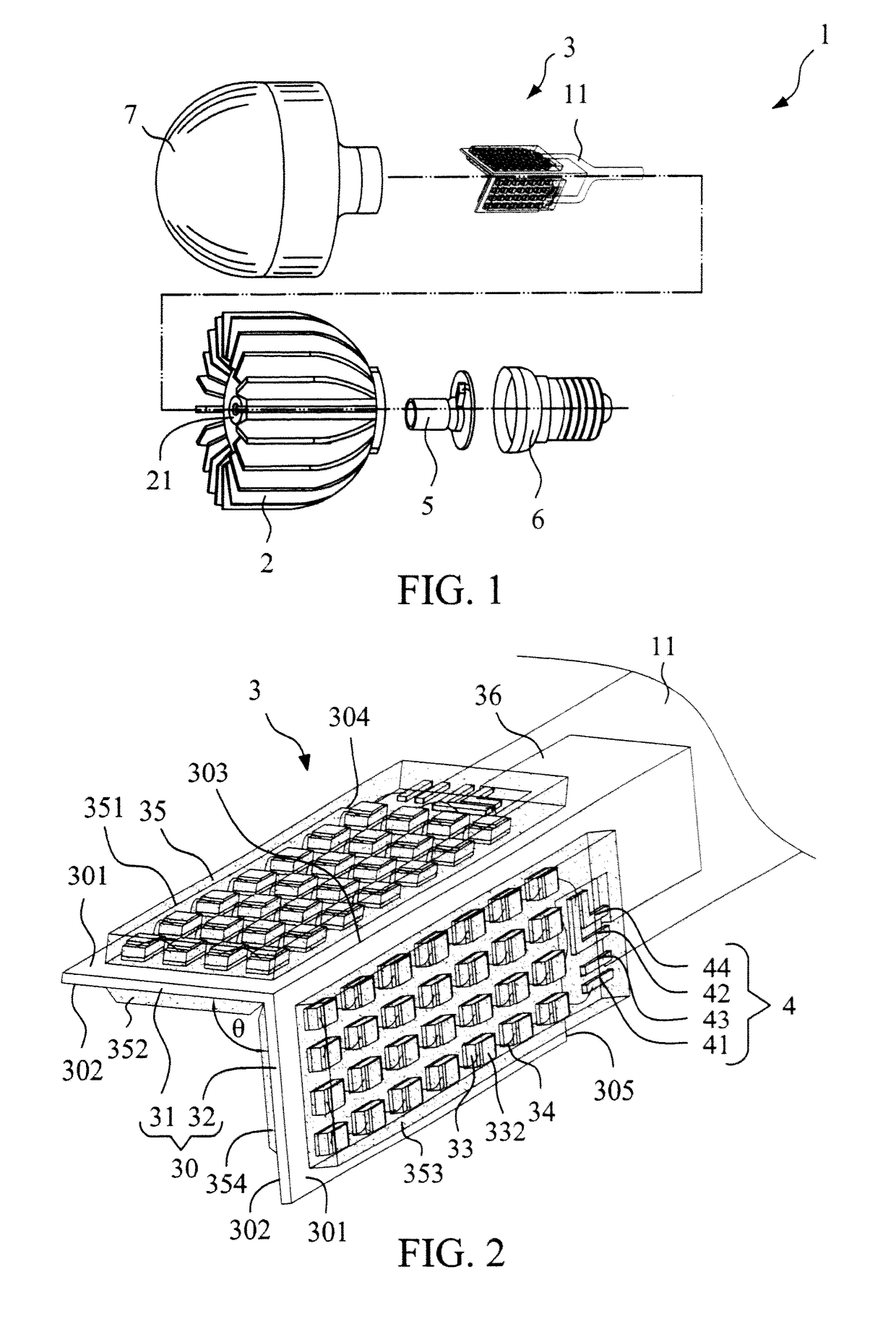
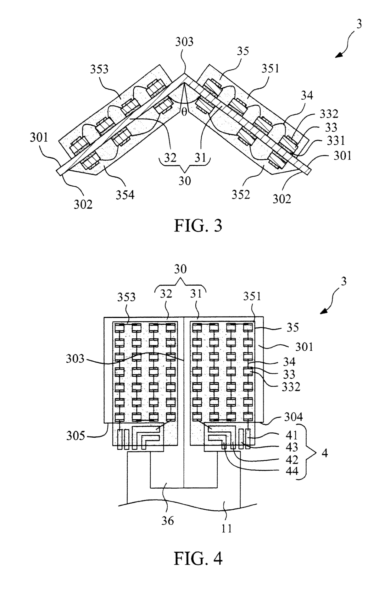
[0020]The light emitting package 3 is connected to the heat sink 2. In this embodiment, the light emitting package 3 is fixed to a rod 11, and the rod 11 is mounted to the heat sink 2 with good thermal contact therebetween. For example, the rod 11 is inserted into and securely attached to the opening 21 of the heat sink 2 using different known methods or materials such as thermally conductive bonding materials or a thermal grease.

[0021]The optical housing 7 is connected or mounted to the heat sink 2 and...


PUM

PropertyMeasurementUnit
inclination angleaaaaaaaaaa
light emitting angleaaaaaaaaaa

Abstract

A light emitting package includes a metal plate, a plurality of LED chips, a plurality of leads and a molding compound. The metal plate has a first surface and a second surface, and is bent into two chip mounting portions, wherein an inclination angle is between the chip mounting portions. The LED chips are mounted on the first surface and the second surface of the chip mounting portions. The leads are disposed adjacent to the metal plate and electrically connected to the LED chips. The molding compound encapsulates the LED chips and a part of the lead.

Description

BACKGROUND OF THE INVENTION[0001]Field of the Invention[0002]The present application relates to a light emitting package and a LED bulb, and more particularly to a light emitting package having a plurality of light emitting diodes and a LED bulb having the same.[0003]Description of the Related Art[0004]A light emitting diode (LED) is widely used in an illumination apparatus for the purpose of high emitting efficiency, small size and saving of electricity. The conventional LED bulb includes a plate substrate and a plurality of LED chips arranged in an array and mounted on the plate substrate. However, the conventional LED bulb has the problem of low light emitting angle. In addition, the plate substrate includes an insulation material therein, thus, the heat dissipating efficiency of the conventional LED bulb is low. Therefore, the application of the conventional LED is limited.SUMMARY OF THE INVENTION[0005]A light emitting diode (LED) bulb includes a first chip mounting portion havi...

Claims


Application Information

Patent Timeline
Patent Type & Authority Patents(United States)
IPC IPC(8): F21V19/00F21V29/77F21K9/23F21Y105/10F21Y105/12F21Y107/00F21Y115/10
CPCF21V19/003F21V29/77F21K9/23F21Y2105/10F21Y2105/12F21Y2107/00F21Y2115/10Y10T29/49002F21Y2107/90
Inventor CHANG, HSIAO-CHUANTSAI, TSUNG-YUEH
Owner ADVANCED SEMICON ENG INC
Why Eureka
Try Eureka