Liquid crystal display device

a liquid crystal display and display device technology, applied in non-linear optics, instruments, optics, etc., can solve the problems of yellowish phenomenon on the display screen, disadvantageous side visibility of the display device, etc., and achieve the effect of maintaining color balan

Active Publication Date: 2017-04-18
SAMSUNG DISPLAY CO LTD
View PDF9 Cites 0 Cited by
  • Summary
  • Abstract
  • Description
  • Claims
  • Application Information

AI Technical Summary

Benefits of technology

[0024]According to embodiments of the present invention, an LCD device may correct chromaticity coordinates by adjusting a cell gap in accordance with a corresponding pixel region using a cell gap adjustment layer, thereby maintaining color balance.

Problems solved by technology

However, the LCD may have disadvantageously lower side visibility than front visibility.
However, the ACC compensation process may cause a yellowish phenomenon on the LCD screen.

Method used


Image

  • Liquid crystal display device
  • Liquid crystal display device
  • Liquid crystal display device

Examples


exemplary embodiment 1

[0042

[0043]Hereinafter, the lower panel 100 will be described.

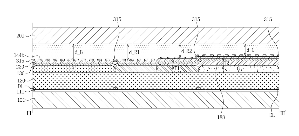
[0044]As illustrated in FIGS. 1 to 3, the lower panel 100 may include a lower substrate 101, a gate line GL, a gate electrode GE, a gate insulating film 111, a semiconductor layer 113, an ohmic contact layer 115, a source electrode SE, a drain electrode DE, a thin film transistor (TFT), a data line DL, a first protective layer 120, a common electrode 130, a cell gap adjustment layer 188, a second protective layer 220, and a pixel electrode 144.

[0045]The lower substrate 101 may be an insulating substrate made of a transparent material, such as glass and / or many plastics.

[0046]The gate line GL and the gate electrode GE may be disposed on the lower substrate 101. Although not illustrated, the gate line GL may have a connecting portion (e.g., an end portion) larger than other portions thereof in size, such that the gate line GL can be connected to another layer or external driving circuits. The gate line GL may be made of met...

exemplary embodiment 2

[0083

[0084]FIG. 6 is a cross-sectional view taken along the line I-I′ of FIG. 1 according to another embodiment of the present invention and FIG. 7 is a cross-sectional view taken along the line II-II′ of FIG. 1 according to another embodiment of the present invention.

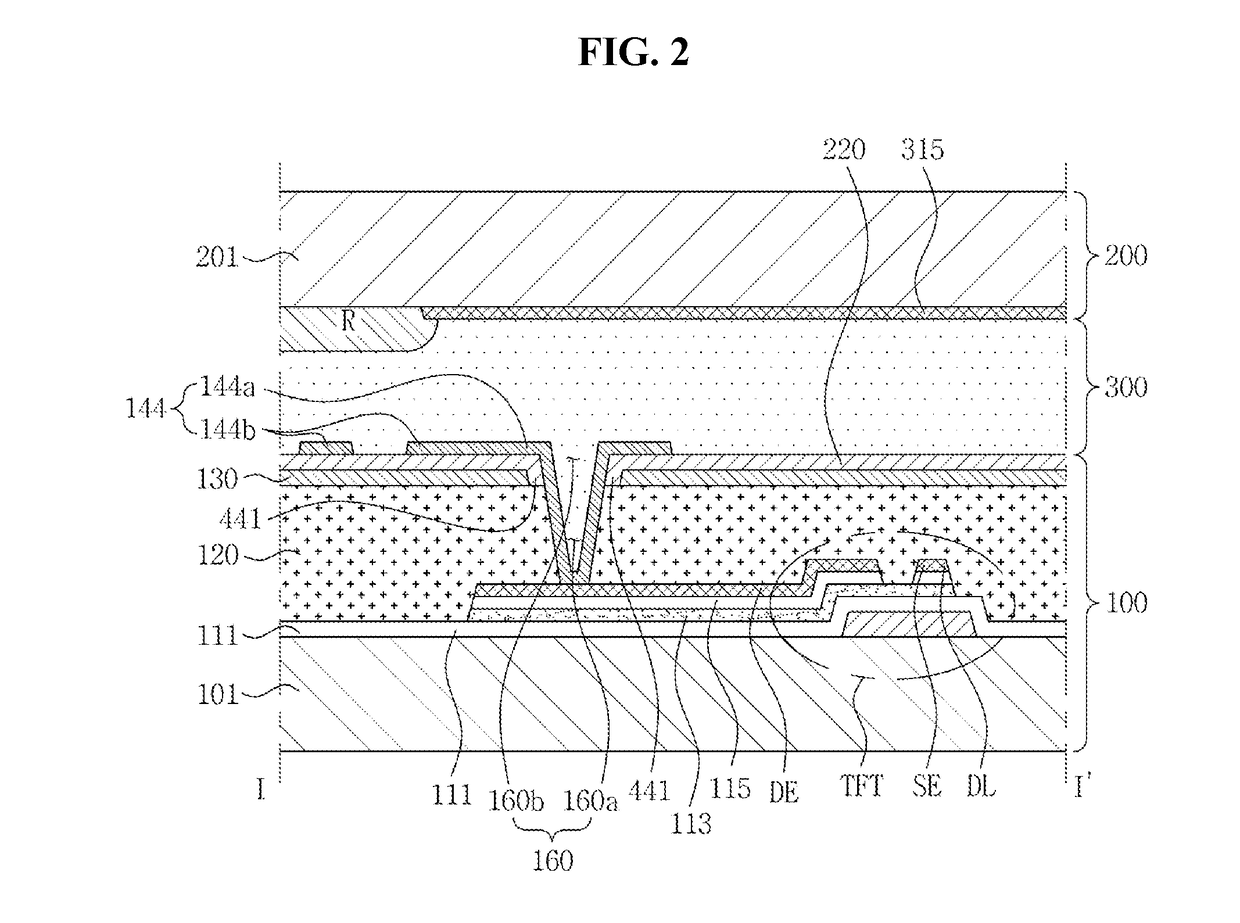
[0085]Referring to FIGS. 1, 6, and 7, an LCD device according to another embodiment of the present invention may include a lower panel 100 and an upper panel 200 disposed to face each other with a liquid crystal layer 300 interposed therebetween.

[0086]As illustrated in FIGS. 1, 6, and 7, the lower panel 100 may include a lower substrate 101, a gate line GL, a gate electrode GE, a gate insulating film 111, a semiconductor layer 113, an ohmic contact layer 115, a source electrode SE, a drain electrode DE, a thin film transistor (TFT), a data line DL, a first protective layer 120, a color filter, a common electrode 130, a cell gap adjustment layer 188, a second protective layer 220, a pixel electrode 144, and a black matr...


PUM

PropertyMeasurementUnit
dielectric constantaaaaaaaaaa
thicknessesaaaaaaaaaa
insulatingaaaaaaaaaa

Abstract

An LCD device includes: a first substrate; a gate line and a data line on the first substrate; at least one TFT connected to the gate and data lines and comprising source and drain electrodes; a pixel electrode connected to the TFT; a second substrate; a liquid crystal layer between the first and second substrates; a common electrode on one of the first and second substrates; a black matrix disposed on one of the first and second substrates and configured to at least partially define a pixel region; a color filter disposed to correspond to the pixel region; and a cell gap adjustment layer disposed on one of the first and second substrates and positioned so as to form different cell gaps within one pixel region.

Description

CROSS-REFERENCE TO RELATED APPLICATION[0001]This application claims priority to, and the benefit of, Korean Patent Application No. 10-2014-0111498, filed on Aug. 26, 2014 with the Korean Intellectual Property Office, the disclosure of which is incorporated herein in its entirety by reference.BACKGROUND[0002]1. Field[0003]Aspects of embodiments of the present invention relate generally to liquid crystal displays. More specifically, aspects of embodiments of the present invention relate to liquid crystal display devices capable of adjusting chromaticity coordinates.[0004]2. Description of the Related Art[0005]A liquid crystal display (LCD) device is a type of flat panel display (FPD) which has found wide recent acceptance. The LCD includes two substrates having electrodes formed thereon and a liquid crystal layer interposed therebetween. Upon applying voltage to the electrodes, liquid crystal molecules of the liquid crystal layer are rearranged, thereby adjusting the amount of transmi...

Claims


Application Information

Patent Timeline
Patent Type & Authority Patents(United States)
IPC IPC(8): G02F1/1335G02F1/1343G02F1/1333
CPCG02F1/133514G02F1/133371G02F1/134363G02F2001/133368G02F2001/134372G02F1/134372G02F1/133368
Inventor PARK, SEUNG HYUNKIM, HYANG YULSONG, JUN HOSONG, JEAN HO
Owner SAMSUNG DISPLAY CO LTD
Why Eureka
Try Eureka