Semiconductor device

a technology of semiconductors and semiconductors, applied in the direction of solid-state devices, instruments, heat measurement, etc., can solve the problems of unusability, cost increase, and inability to operate conventionally used temperature detecting elements such as photodiodes, and achieve the effect of improving assemblability and cost reduction

Active Publication Date: 2017-04-18
MITSUBISHI ELECTRIC CORP
View PDF27 Cites 0 Cited by
  • Summary
  • Abstract
  • Description
  • Claims
  • Application Information

AI Technical Summary

Benefits of technology

[0007]An object of the present invention is to obtain a semiconductor device in which a temperature detecting function of a wide gap semiconductor element is operated normally, and to achieve cost reduction and improvement in assemblability.
[0011]In addition, the photodiode is provided in a form so as to receive the emitted light obtained by propagation through the optical fiber. With this configuration, therefore, the photodiode is not required to be provided integrally with the semiconductor element, so that a formation area of a semiconductor element forming portion forming the semiconductor element can be reduced to achieve cost reduction and improvement in assemblability.
[0012]In addition, in a case when a formation area of a wide gap semiconductor element forming portion is formed in the same size as the conventional technique, a greater effective area of the wide gap semiconductor element can be obtained as compared to that of the conventional technique, so that properties of the wide gap semiconductor element itself can be improved.
[0013]Further, the temperature detecting portion (photodiode) which is electrically weak is not required to be formed integrally with the semiconductor element, so that the reliability of the semiconductor device can be improved.

Problems solved by technology

Consequently, there have been disadvantages in forming a pad portion for transmitting and receiving a signal between the temperature detecting element and the outside.
This configuration increases a device (chip) area to lead to cost increase, and requires an excessive wire bonding process in the pad portion to impose a greater constraint on assembling of the semiconductor device.
In addition, in a case of a wide gap semiconductor element in which a power semiconductor element is formed of a wide gap semiconductor material having light-emitting property, there has been a problem in that when the wide gap semiconductor element is operated at a high temperature of 200° C. or higher intended during the operation thereof, the conventionally used temperature detecting element such as a photodiode does not operate and is unusable.

Method used


Image

  • Semiconductor device
  • Semiconductor device
  • Semiconductor device

Examples


Embodiment Construction
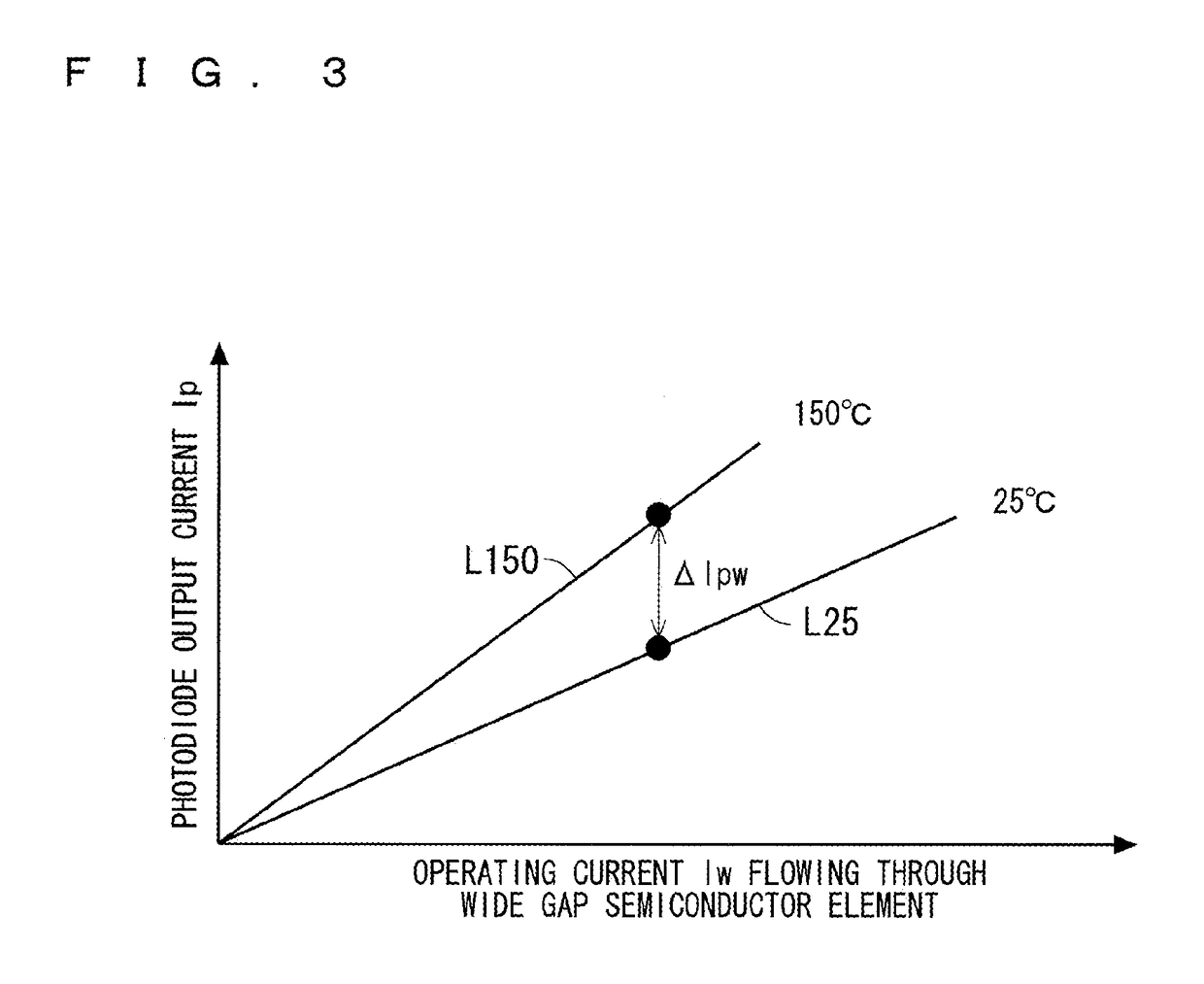
[0024]

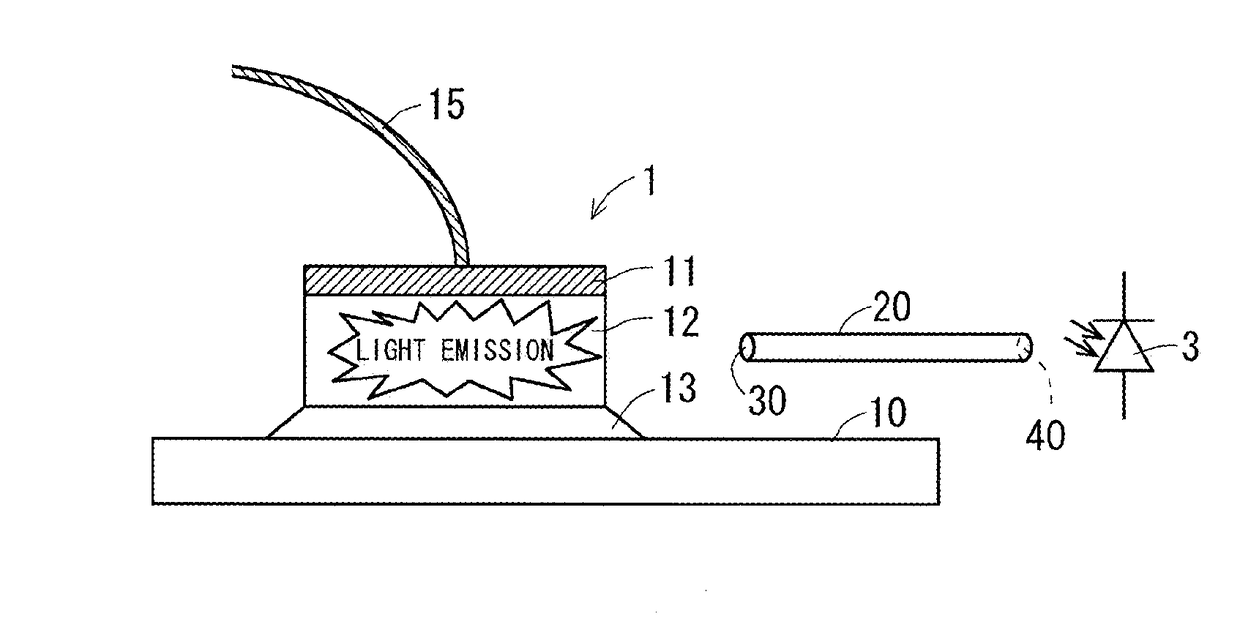
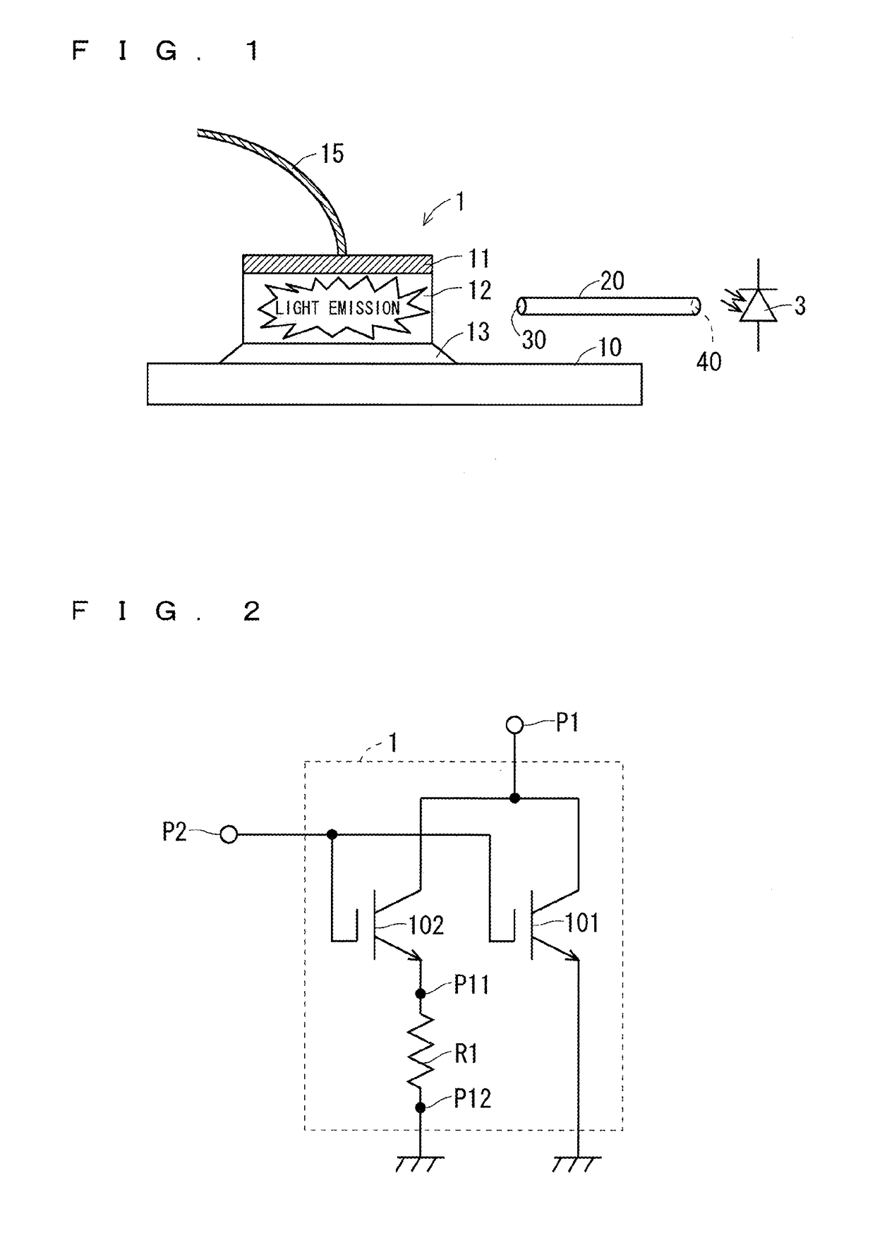
[0025]FIG. 8 is an explanatory view schematically showing a planar configuration of a conventional semiconductor device having a temperature detecting function. As shown in FIG. 8, a surface electrode 51 of a main electrode (serving as a collector electrode) of an IGBT (Insulated Gate Bipolar Transistor) is formed in a majority of a region on a substrate 50, and a gate electrode 53 of the IGBT is formed in a part of the surface electrode 51. Then, a current sensing portion 52 (current sensing main portion 52M and pad portion 52P) is formed in a part other than the gate electrode 53, and a temperature sensing portion 54 (temperature sensing main portion 54M and pad portion 54P) is formed in a part other than the gate electrode 53 and the current sensing portion 52. Note that, a sensing IGBT (main electrode, i.e., collector electrode), for example, is formed in the current sensing main portion 52M, and a photodiode, for example, is formed in a temperature sensing main portion 54...


PUM

PropertyMeasurementUnit
temperatureaaaaaaaaaa
operating temperatureaaaaaaaaaa

Abstract

An optical fiber is provided between a photodiode and a semiconductor active portion of a wide gap semiconductor element forming portion such that emitted light at the time of light emission of the semiconductor active portion of the wide gap semiconductor element forming portion is incident from an incident surface of the optical fiber, and is received from an emitting surface to the photodiode through the optical fiber. Specifically, the incident surface of the optical fiber is arranged so as to be opposed to a side surface portion of the wide gap semiconductor element forming portion, so that the emitted light at the time of light emission of the wide gap semiconductor element is incident on the incident surface.

Description

BACKGROUND OF THE INVENTION[0001]Field of the Invention[0002]The present invention relates to a semiconductor device which has a wide gap semiconductor element and which is capable of detecting a temperature of the wide gap semiconductor element.[0003]Description of the Background Art[0004]Conventionally, for measuring an operating temperature of a power semiconductor element, there has been generally used a semiconductor device having a power semiconductor element. The semiconductor device has a temperature detecting element such as a polysilicon diode formed therein electrically independently from the power semiconductor element to detect temperature of the power semiconductor element by temperature characteristics of the temperature detecting element. As a semiconductor device of this type, there is, for example, a current conversion device disclosed in Japanese Patent Application Laid-Open No. 2006-271098.[0005]In a conventional semiconductor device which has a temperature detec...

Claims


Application Information

Patent Timeline
Patent Type & Authority Patents(United States)
IPC IPC(8): H01L31/16H01L31/167G01K7/01
CPCH01L31/167G01K7/01G01K2217/00H01L2224/48091H01L2224/73265H01L2924/12032H01L2924/13055H01L2924/00014H01L2924/00
Inventor KAGUCHI, NAOTOTARUI, YOICHIRO
Owner MITSUBISHI ELECTRIC CORP
Why Eureka
Try Eureka