Semiconductor package and method of manufacturing the same
a technology of semiconductor and packaging, applied in the direction of semiconductor/solid-state device details, semiconductor devices, electrical apparatus, etc., can solve the problems of fine pitch patterning, limit in selecting insulating materials,
- Summary
- Abstract
- Description
- Claims
- Application Information
AI Technical Summary
Benefits of technology
Problems solved by technology
Method used
Image

Examples
first embodiment
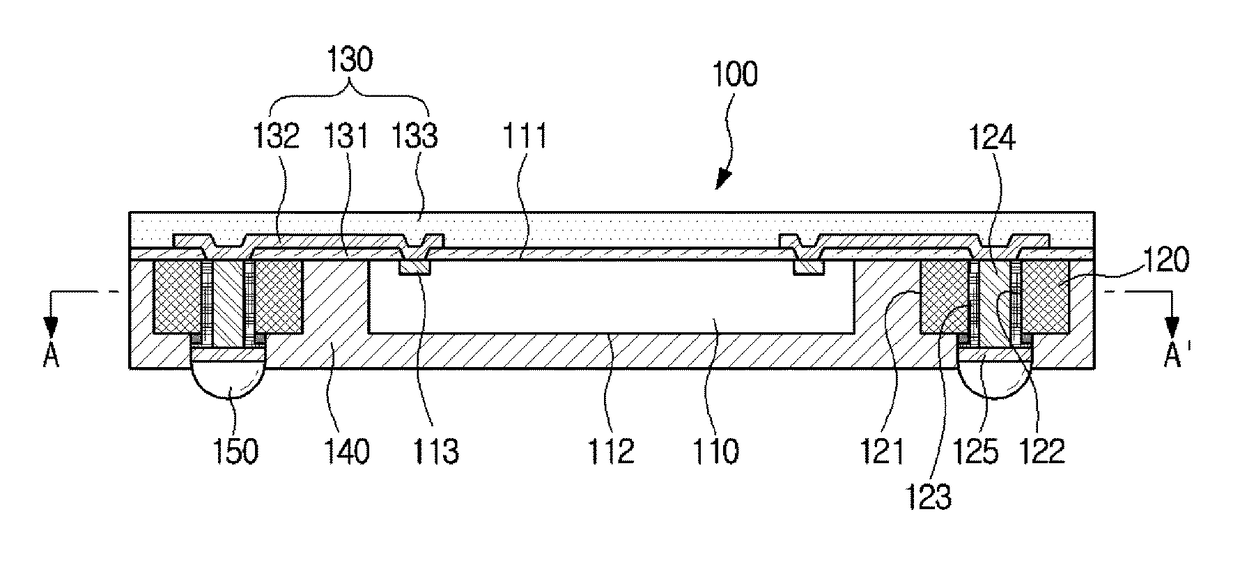
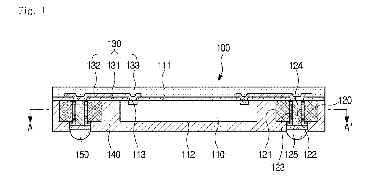
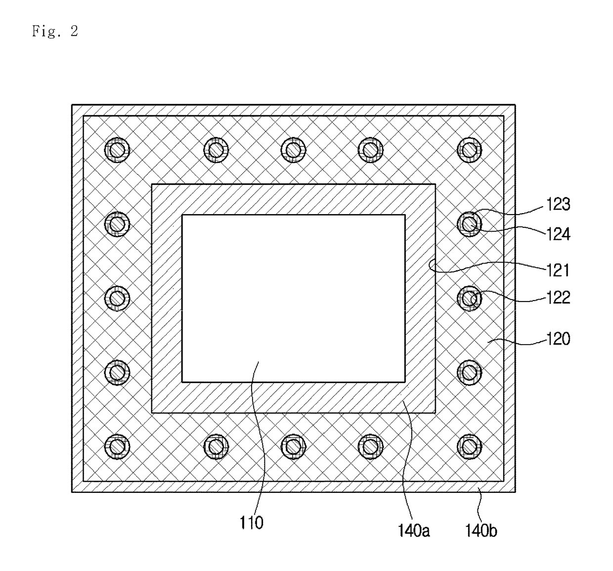
[0043]A semiconductor package 100 according to an embodiment of the present invention will be described referring to FIGS. 1 to 4. FIG. 1 is a cross-sectional view of the semiconductor package 100 according to the embodiment of the present invention. FIG. 2 is a plan view taken along line A-A of the semiconductor package 100 in FIG. 1. FIG. 3 is a plan view of illustrating a substrate according to another embodiment of the present invention. FIG. 4 is an enlarged view illustrating a structure in which a through wiring 123 is coupled with a wiring layer 132 according to the present invention.
[0044]The semiconductor package 100 according to the embodiment of the present invention may include a substrate 120, a semiconductor chip 110 accommodated on the substrate 120, a through wiring 123 provided in an outer side of a semiconductor chip 110, a wiring portion 130 which electrically connect the semiconductor chip 110 with the through wiring 123, an external connection portion 150 connec...
second embodiment
[0079]FIG. 5 is an enlarged view illustrating a structure in which a through wiring 123 is coupled with a wiring layer 132-1 according to the present invention.
[0080]Referring to FIG. 5, the first insulating layer 131-1 may be formed to fully expose a through wiring 123. An opening in the first insulating layer 131-1 is provided to connect the wiring layer 132-1 and the through wiring 123. The width of the opening may be provided to be greater than the outer diameter of a via hole 122 of a substrate 120. Since the wiring layer 132-1 fills up the opening of the first insulating layer 131-1 in a process of forming patterns, all end portions of the through wiring 123 are in contact with the wiring layer 132-1. Comparatively referring to FIGS. 4 and 5, the contact areas of the through wiring 123 and the wiring layer 132-1 are different. When the contact area of the through wiring 123 and the wiring layer 132-1 become larger, the reliability of transmitting electrical signals may be enha...
third embodiment
[0081]FIG. 6 is an enlarged view illustrating a structure in which a through wiring 123-1 is coupled with a wiring layer 132 according to the present invention.
[0082]Referring to FIG. 6, the through wiring 123-1 may be provided to fill a via hole 122. For example, the through wiring 123-1 may be a conductive paste to fill the via hole 122. By using a conductive paste as the through wiring 123-1 according to the third embodiment of the present invention, the manufacturing cost can be reduced and the manufacturing process can be simplified.
[0083]FIGS. 7 to 21 are cross-sectional views illustrating a manufacturing process of the semiconductor package 100 according to the embodiment of the present invention.
[0084]FIG. 7 illustrates a process in which a substrate 120 in which an accommodating portion 121 is formed is provided. The substrate 120 may include an insulating material such as silicon, glass, a ceramic, a plastic, or a polymer. The substrate 120 may be provided to have a plate ...
PUM
 Abstract
Description
Claims
Application Information
 - R&D
- Intellectual Property
- Life Sciences
- Materials
- Tech Scout
- Unparalleled Data Quality
- Higher Quality Content
- 60% Fewer Hallucinations
Browse by: Latest US Patents, China's latest patents, Technical Efficacy Thesaurus, Application Domain, Technology Topic, Popular Technical Reports.
© 2025 PatSnap. All rights reserved.Legal|Privacy policy|Modern Slavery Act Transparency Statement|Sitemap|About US| Contact US: help@patsnap.com