Liquid crystal device, method of manufacturing liquid crystal device, and electronic apparatus
a liquid crystal device and liquid crystal technology, applied in liquid crystal compositions, chemistry apparatus and processes, instruments, etc., can solve problems such as reliability deterioration, display quality lowering, display quality affecting, etc., and achieve the effect of suppressing display quality
- Summary
- Abstract
- Description
- Claims
- Application Information
AI Technical Summary
Benefits of technology
Problems solved by technology
Method used
Image

Examples
first embodiment
Configuration of Liquid Crystal Device
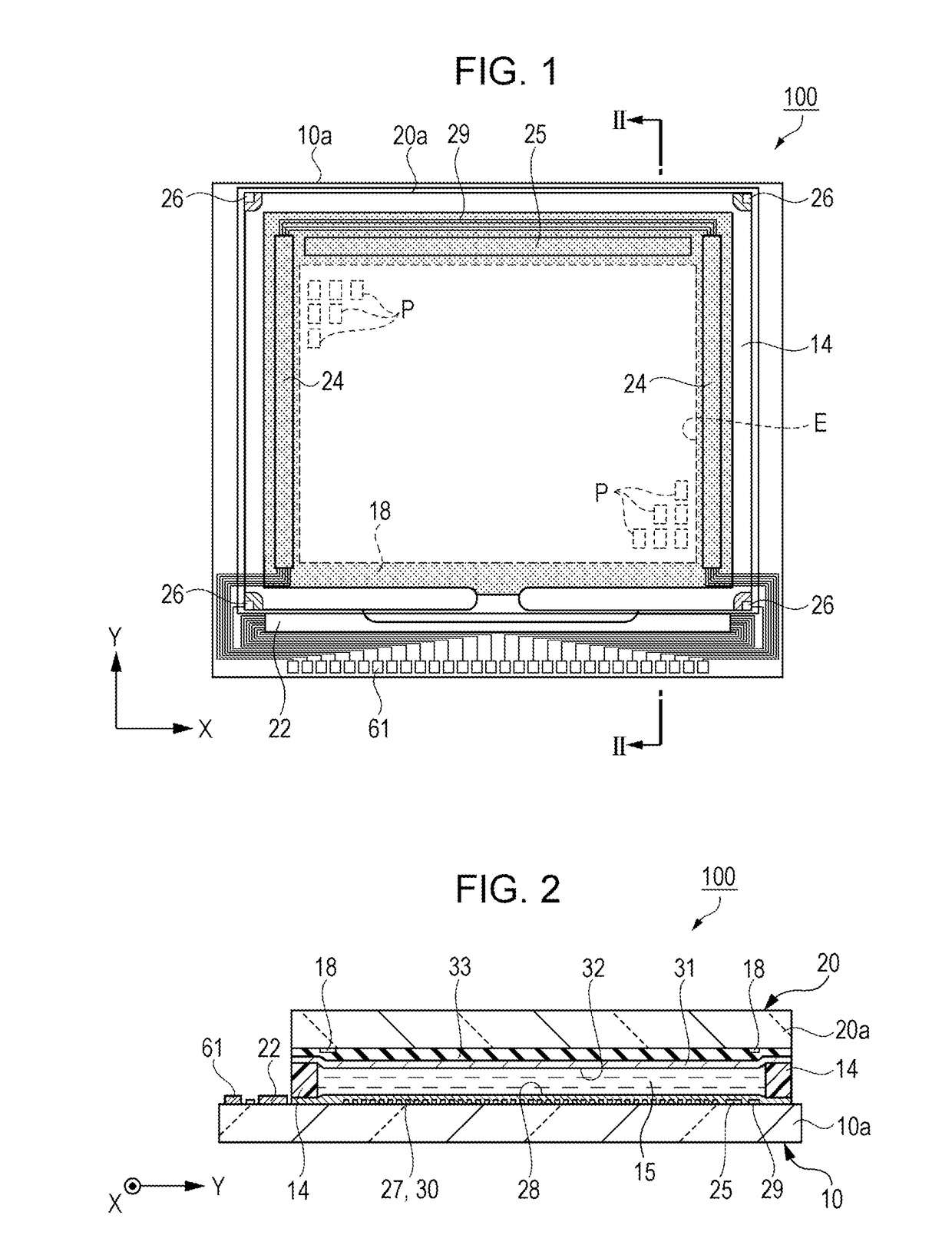
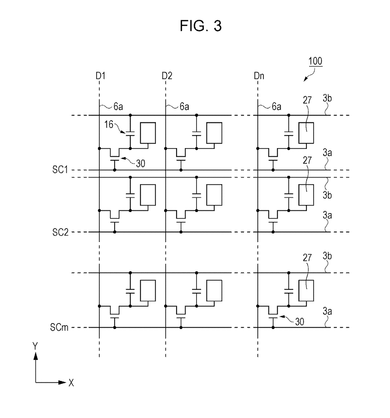
[0036]FIG. 1 is a schematic plan diagram illustrating the configuration of a liquid crystal device. FIG. 2 is a schematic cross-sectional diagram taken along line II-II of the liquid crystal device shown in FIG. 1. FIG. 3 is an equivalent circuit diagram illustrating the electrical configuration of the liquid crystal device. Hereinafter, the configuration of the liquid crystal device will be described with reference to FIGS. 1 to 3.
[0037]As shown in FIGS. 1 and 2, a liquid crystal device 100 according to the embodiment includes an element substrate 10 (first substrate) and a counter substrate 20 (second substrate) which are arranged to face each other, and a liquid crystal layer 15 which is interposed between the pair of substrates.
[0038]The element substrate 10 is larger than the counter substrate 20, and both substrates are connected to each other while interposing a sealing material 14 which is arranged along the outer circumference of the co...
second embodiment
Configuration of Liquid Crystal Device and Method of Manufacturing Liquid Crystal Device
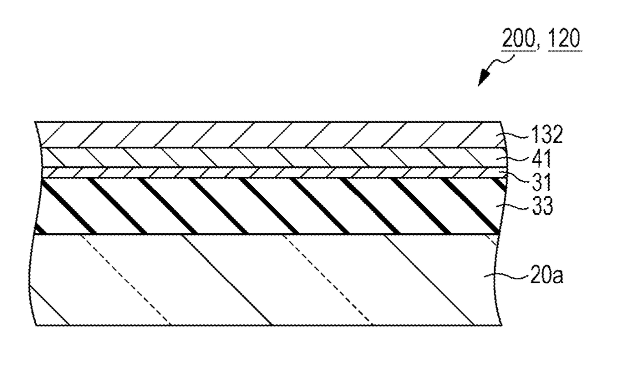
[0111]FIG. 11 is a schematic cross-sectional diagram illustrating the structure of a liquid crystal device (counter substrate) according to a second embodiment. Hereinafter, the structure of the liquid crystal device will be described with reference to FIG. 11.
[0112]The liquid crystal device 200 according to the second embodiment is different from the above-described liquid crystal device 100 according to the first embodiment in that the film 41 (second film) of the silane compound, with which the fullerenes are modified, is arranged on the base of an alignment film 132 (second alignment film, and the side of the element substrate corresponds to the first alignment film), and the other parts are generally similar to the liquid crystal device 100 according to the first embodiment. Therefore, in the second embodiment, parts which are different from the first embodiment will be described in detail a...
third embodiment
Configuration of Liquid Crystal Device and Method of Manufacturing Liquid Crystal Device
[0119]FIG. 12 is a schematic cross-sectional diagram illustrating the structure of a liquid crystal device (counter substrate) according to a third embodiment. FIG. 13 is a flowchart illustrating a method of manufacturing the liquid crystal device in process order. Hereinafter, the structure of the liquid crystal device according to the third embodiment and the method of manufacturing the liquid crystal device will be described with reference to FIGS. 12 and 13. Meanwhile, FIG. 12 illustrates only the counter substrate similarly to the first embodiment and the second embodiment.
[0120]A liquid crystal device 300 according to the third embodiment is different from the liquid crystal device 100 according to the first embodiment in that the alignment film is an organic alignment film 232 and the organic alignment film 232 includes the fullerenes, and the other parts are generally similar to the liqui...
PUM
| Property | Measurement | Unit |
|---|---|---|
| adhesion | aaaaa | aaaaa |
| orientation regulation force | aaaaa | aaaaa |
| electrical configuration | aaaaa | aaaaa |
Abstract
Description
Claims
Application Information
 - R&D
- Intellectual Property
- Life Sciences
- Materials
- Tech Scout
- Unparalleled Data Quality
- Higher Quality Content
- 60% Fewer Hallucinations
Browse by: Latest US Patents, China's latest patents, Technical Efficacy Thesaurus, Application Domain, Technology Topic, Popular Technical Reports.
© 2025 PatSnap. All rights reserved.Legal|Privacy policy|Modern Slavery Act Transparency Statement|Sitemap|About US| Contact US: help@patsnap.com