Active matrix substrate, liquid crystal panel, liquid crystal display device, liquid crystal display unit, and television receiver

a technology of liquid crystal display device and active matrix substrate, which is applied in the direction of semiconductor devices, instruments, computing, etc., can solve the problems of complicated design, and deterioration of flexibility of product use, so as to suppress the deterioration of display quality

Inactive Publication Date: 2011-01-27
SHARP KK
View PDF3 Cites 13 Cited by
  • Summary
  • Abstract
  • Description
  • Claims
  • Application Information

AI Technical Summary

Benefits of technology

0019] According to a liquid crystal display device including the present active matrix substrate, the pixel electrodes in a single pixel region are connected to a data signal line via respective transistors which are connected to respective different scanning signal lines. This makes it possible to supply signal electric potentials to respective pixel electrodes at different timings. Accordingly, for example, before a signal electric potential for regular writing is supplied to one of the pixel electrodes, a signal electric potential (e.g., Vcom) can be supplied to the other of the pixel electrodes which (i) is capacitor-connected to the one of the pixel electrodes and (ii) is electrically connected to the data signal line via a transistor.
0020] With the configuration, before regular writing is carried out, a signal electric potential can be supplied via the data signal line, not via a capacitor, to a pixel electrode (capacitor-coupled electrode) which is coupled, via capacitor, with a pixel electrode connected to the signal line via a transistor. This makes it possible to discharge (refresh) electric charge stored in the capacitor-coupled electrode. Accordingly, image-sticking in a sub-pixel including the pixel electrode can be prevented. Moreover, according to the configuration, it is not necessary to adjust W / L ratios of respective channels of the transistors unlike a conventional configuration, and the active matrix substrate can be configured with channel sizes identical to each other. This makes it possible to suppress deterioration of display quality due to variation in characteristics of transistors.

Problems solved by technology

This may cause the design to be complicated.
Moreover, after the liquid crystal panel is made, it is difficult to adjust, for example, time for writing into each pixel electrode, and whereby flexibility of usage of the product is deteriorated.
This may cause deterioration of display quality because the characteristics of the first and second transistors are different from each other in a display screen.

Method used


Image

  • Active matrix substrate, liquid crystal panel, liquid crystal display device, liquid crystal display unit, and television receiver
  • Active matrix substrate, liquid crystal panel, liquid crystal display device, liquid crystal display unit, and television receiver
  • Active matrix substrate, liquid crystal panel, liquid crystal display device, liquid crystal display unit, and television receiver

Examples


embodiment 1

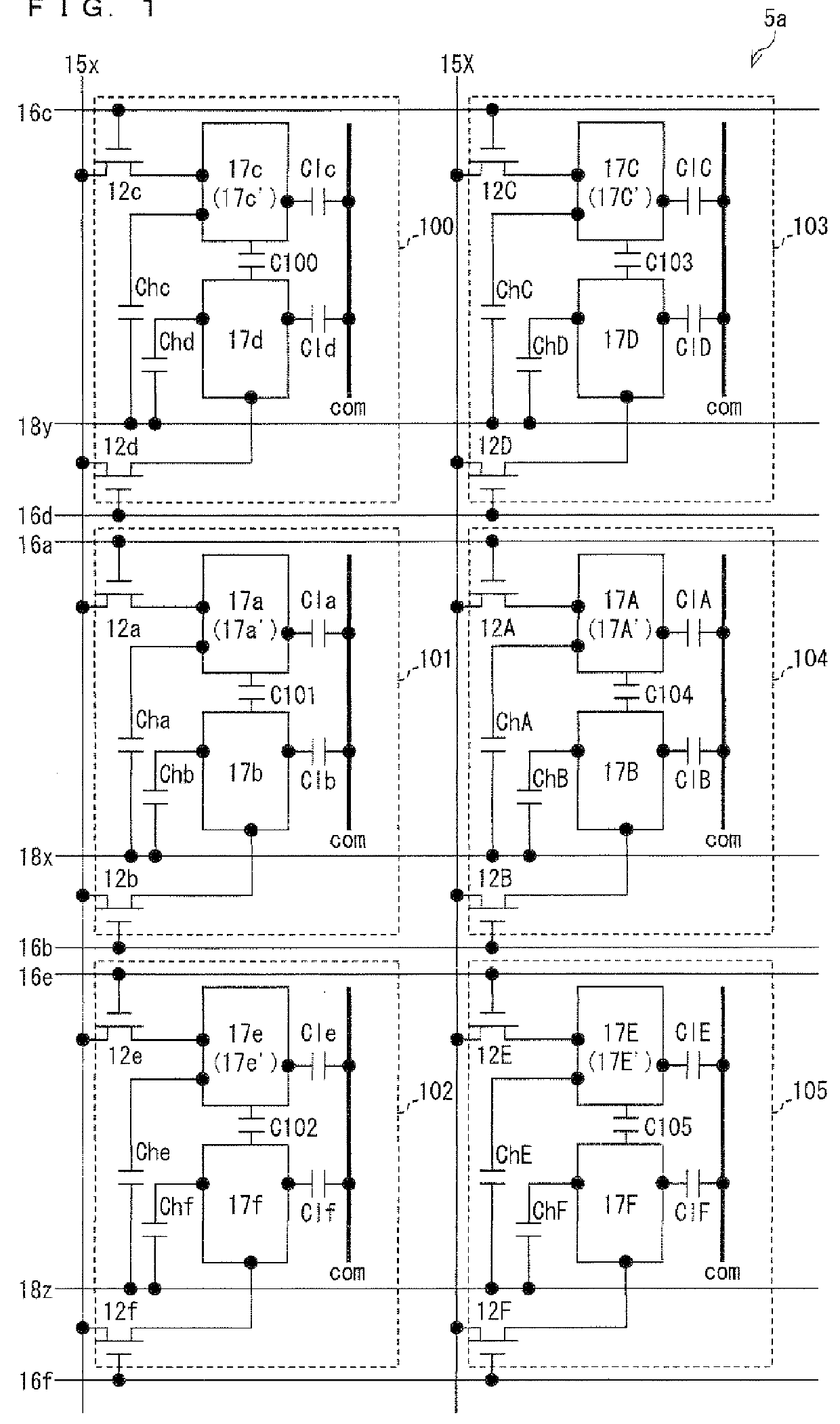
[0150] FIG. 1 is an equivalent circuit diagram illustrating part of a liquid crystal panel of the present embodiment 1. As shown in FIG. 1, a liquid crystal panel 5a includes: data signal lines (15x and 15X) that extend in a column direction (vertical direction in FIG. 1); scanning signal lines (16a through 16f) that extend in a row direction (horizontal direction in FIG. 1); pixels (100 through 105) that are provided in the row and column directions; storage capacitor wires (18x through 18z); and a common electrode (counter electrode) com. The pixels are configured in an identical manner. Note that a pixel array including the pixels 100 through 102 is adjacent to a pixel array including the pixels 103 through 105.

[0151] According to the liquid crystal panel 5a, one (1) data signal line and two scanning signal lines are provided for each of the pixels. Two pixel electrodes 17c and 17d are provided in the pixel 100, two pixel electrodes 17a and 17b are provided in the pixel 101, and ...

concrete example 1-1

of Liquid Crystal Panel

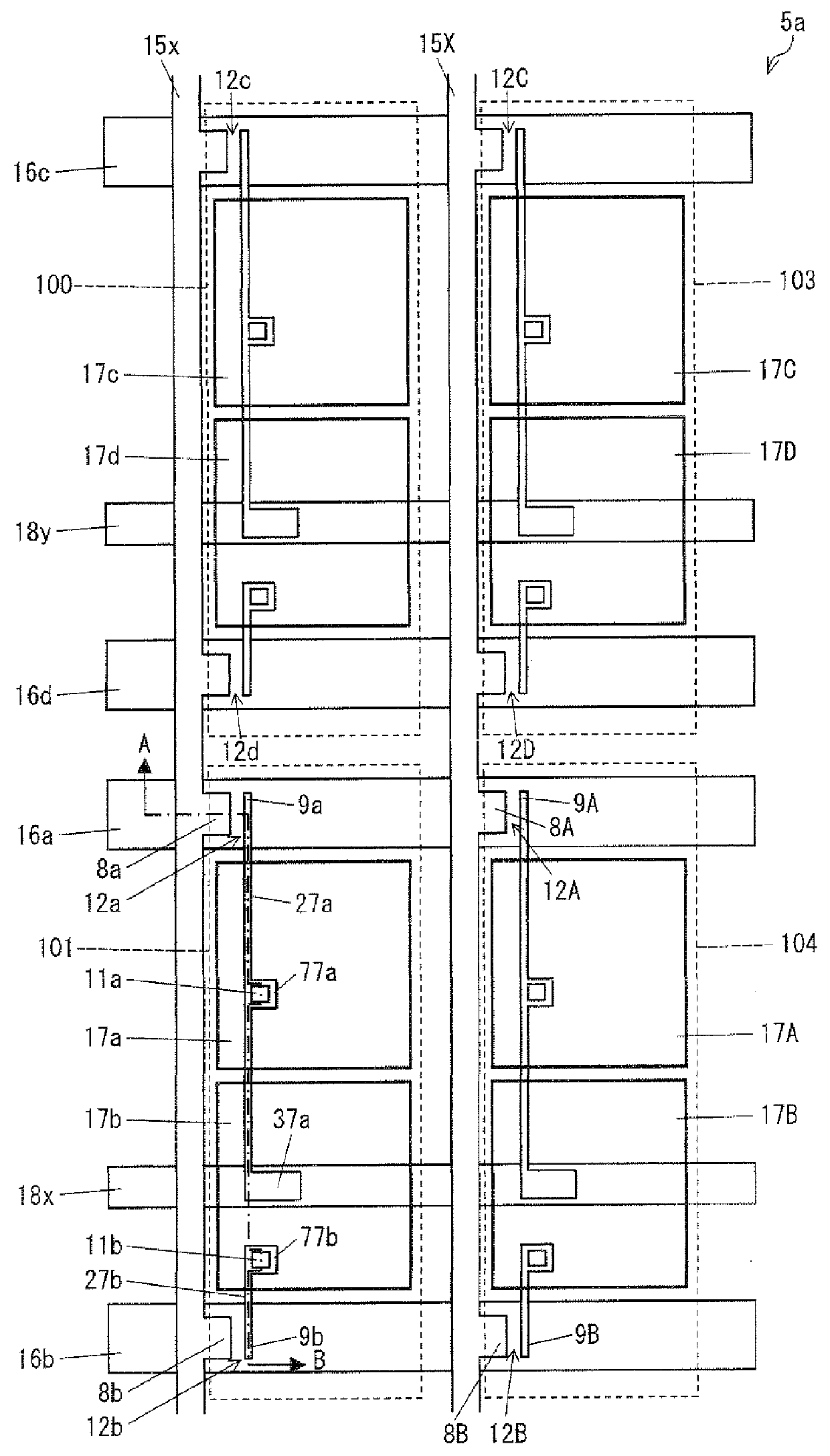
[0160] FIG. 2 illustrates a concrete example 1-1 of the liquid crystal panel 5a. According to the liquid crystal panel 5a shown in FIG. 2, a data signal line 15x is provided along a pixel 100 and a pixel 101; a data signal line 15X is provided along a pixel 103 and a pixel 104; a storage capacitor wire 18y is provided so as to traverse the pixels 100 and 103; and a storage capacitor wire 18x is provided so as to traverse the pixels 101 and 104.

[0161] In the liquid crystal panel 5a, a scanning signal line 16c is provided so that the scanning signal line 16c and one of two edge parts of the pixel 100 overlap each other, which two edge parts extend in the row direction; a scanning signal line 16d is provided so that the scanning signal line 16d and the other of the two edge parts overlap each other; and pixel electrodes 17c and 17d are juxtaposed in the column direction between the scanning signal lines 16c and 16d when they are viewed from above. The scanning si...

concrete example 1-2

of Liquid Crystal Panel

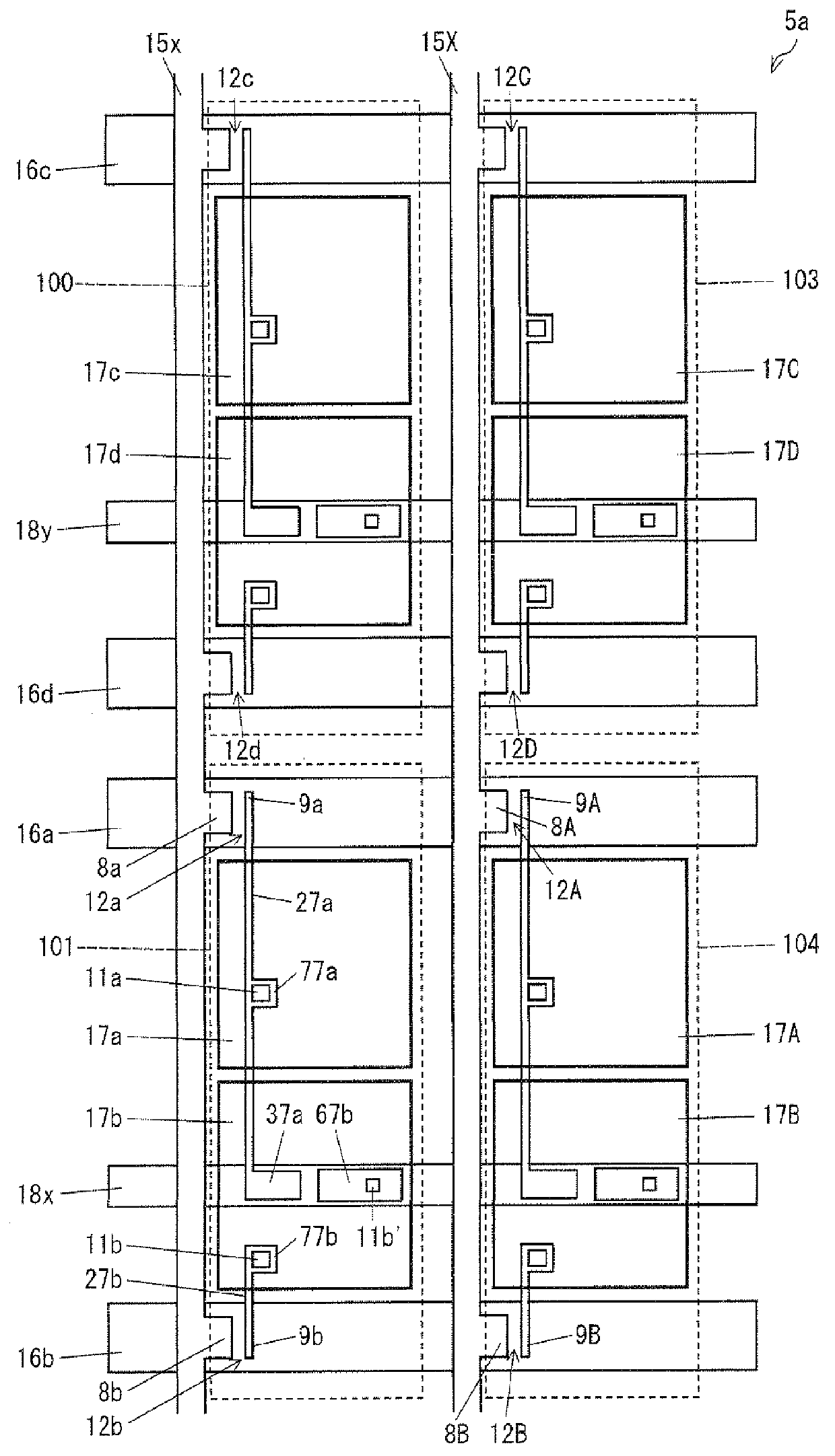
[0181] FIG. 6 illustrates a concrete example 1-2 of the liquid crystal panel 5a. According to the liquid crystal panel 5a shown in FIG. 6, three pixel electrodes are provided in each pixel region. Further, according to the liquid crystal panel 5a shown in FIG. 6, as with the liquid crystal panel shown in FIG. 2, a data signal line 15x is provided along a pixel 100 and a pixel 101; a data signal line 15X is provided along a pixel 103 and a pixel 104; a storage capacitor wire 18y is provided so as to traverse the pixels 100 and 103; and a storage capacitor wire 18x is provided so as to traverse the pixel 101 and 104.

[0182] In the liquid crystal panel 5a, a scanning signal line 16c is provided so that the scanning signal line 16c and one of two edge parts of the pixel 100 overlap each other, which two edge parts extend in the row direction; a scanning signal line 16d is provided so that the scanning signal line 16d and the other of the two edge parts overlap each...


PUM

PropertyMeasurementUnit
thicknessaaaaaaaaaa
thicknessaaaaaaaaaa
thicknessaaaaaaaaaa

Abstract

Provided are an active matrix substrate including plural pixel electrodes in a pixel region and a liquid crystal display device (pixel division mode) using the same. Proposed is a configuration of the liquid crystal display device of the capacitor-coupled pixel division mode which hardly causes reduction in display quality due to image-sticking of sub-pixels. The active matrix substrate includes: a data signal line (15x); scanning signal lines (16a and 16b); a transistor (12a) connected to the data signal line (15x) and scanning signal line (16a); a transistor (12b) connected to the data signal line (15x) and scanning signal line (16b); and pixel electrodes (17a and 17b) provided in a pixel region (101), the pixel electrode (17a) being connected to the data signal line (15x) via the transistor (12a), the pixel electrode (17b) being connected to the pixel electrode (17a) via a capacitor and the data signal line (15x) via the transistor (12b), and the transistors (12a and (12b) have identical W/L ratios of channels (each ratio of width W to length L of channel). The present invention can be configured with identical channel sizes without adjusting W/L ratios of channels of the transistors unlike a conventional configuration. Accordingly, deterioration of display quality due to variation in characteristics of transistors can be suppressed.

Description

[0001] The present invention relates to an active matrix substrate including a plurality of pixel electrodes in a pixel region, and a liquid crystal display device (pixel division mode) including the same.[0002] As a measure for improving viewing angle dependence of gamma characteristics in liquid crystal display devices (for example, holding down excess brightness and the like in a screen), a liquid crystal display device has been proposed which controls a plurality of sub-pixels in one pixel to have different brightness, so as to display a halftone by area coverage modulation of these sub-pixels (pixel division mode; for example, see Patent Literature 1).[0003] As shown in FIG. 44, an active matrix substrate disclosed in Patent Literature 1 has a pixel region provided between two adjacent gate bus lines 112; a pixel electrode 121a disposed in an upper end part (part adjacent to one of the two gate bus lines) of the pixel region; a pixel electrode 121b disposed midway of the pixel ...

Claims


Application Information

Patent Timeline
Patent Type & Authority Applications(United States)
IPC IPC(8): G02F1/1343G09G5/00G02F1/136
CPCG02F1/13624H01L29/78696H01L27/1296
Inventor TSUBATA, TOSHIHIDE
Owner SHARP KK
Why Eureka
Try Eureka