Ink cartridge, ink cartridge chip, and short-circuit detection method of chip
a technology of ink cartridges and chips, applied in the field of short-circuit self-detection technology of chips, can solve the problems of short-circuit, damage to storage units, damage to ink cartridges or recording devices, etc., and achieve the effect of low cost and durabl
- Summary
- Abstract
- Description
- Claims
- Application Information
AI Technical Summary
Benefits of technology
Problems solved by technology
Method used
Image
Examples
embodiment 1
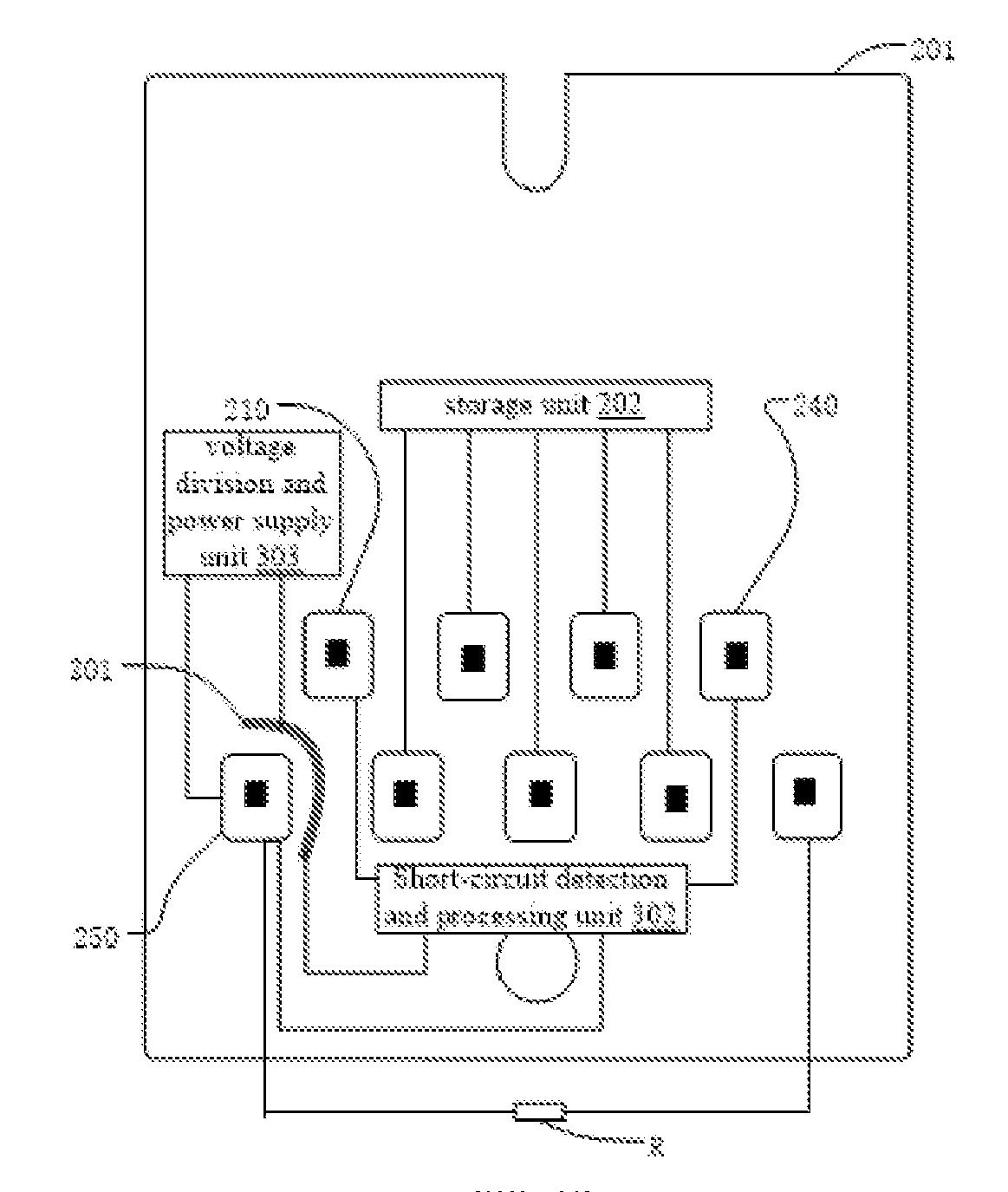
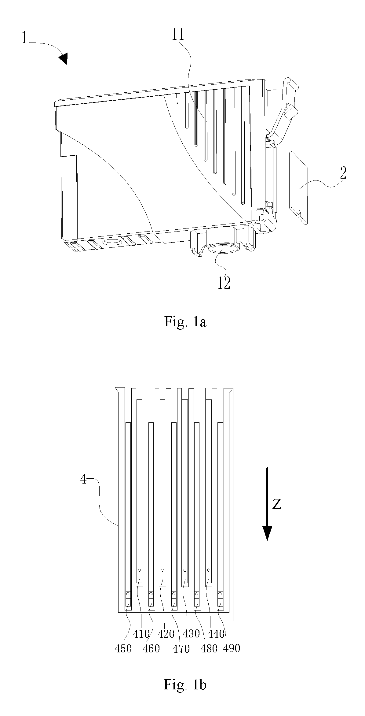
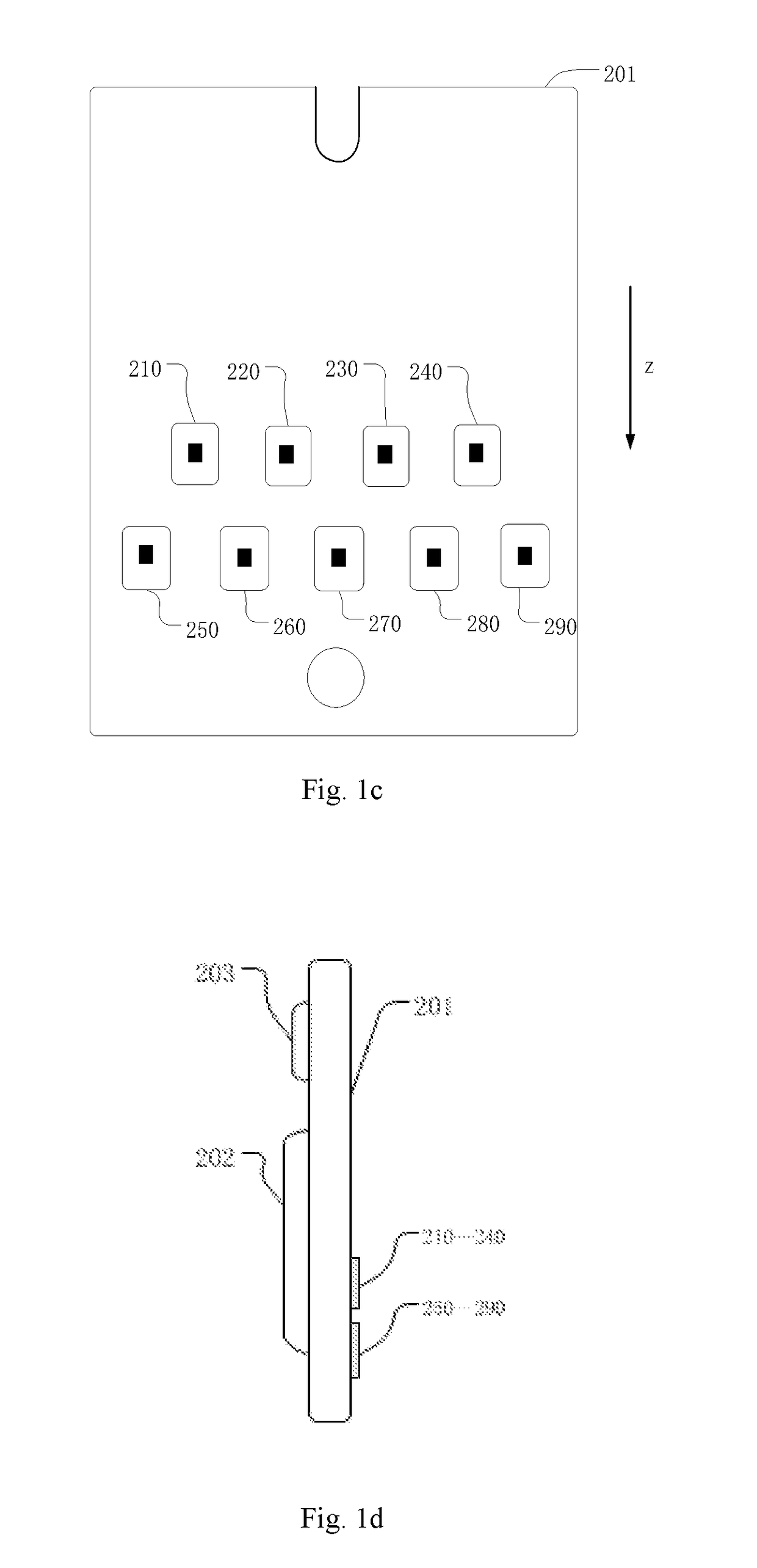
[0057]FIG. 1a schematically shows structure of an ink cartridge applicable to a chip provided in the present embodiment. FIG. 1b schematically shows arrangement structure of device-side terminals of an ink-jet printer applicable to the ink cartridge as shown in FIG. 1a. FIG. 1c schematically shows a front view of structure of the chip provided in the present embodiment. FIG. 1d schematically shows a side view of structure of the chip provided in the present embodiment. FIG. 1e schematically shows structure of a circuit of the chip provided in the present embodiment. FIG. 1f schematically shows structure of mounting the ink cartridge applicable to the present embodiment to a corresponding printer.
[0058]As shown in FIG. 1a, the ink cartridge 1 comprises: a body 11, for storing ink used for printing; an ink supply part 12, which is formed on a bottom wall of the body 11, and is connected to an ink supply tube when the ink cartridge 1 is mounted into the ink-jet printer so as to deliver...
embodiment 2
[0079]FIG. 4a schematically shows a front view of structure of a chip according to the present embodiment; FIG. 4b schematically shows a side view of structure of the chip according to the present embodiment; and FIG. 4c schematically shows structure of a circuit of the chip according to the present embodiment.
[0080]The present embodiment provides a chip. As shown in FIG. 4b, the chip comprises a circuit board 701, a storage unit 702, and a second electrical element 703. The circuit board 701 is provided thereon with two rows of connecting terminals, preferably. The storage unit 702 is used for storing information about the ink cartridge. The second electrical element 703 may also be provided on the ink cartridge on which the chip is arranged. The second electrical element 703 may be a piezoelectric sensor, or a resistor element.
[0081]As shown in FIG. 4a, the connecting terminals on the circuit board 701 of the chip are arranged in two lines, and respectively are connecting terminal...
embodiment 3
[0089]FIG. 5 schematically shows structure of circuits of a short-circuit detection device of chip according to the present embodiment. The two circuits respectively show circuit structure of a short-circuit detection and processing unit and circuit structure of a voltage division and power supply unit. One skilled person in the art should understand that said short-circuit detection device of chip can be formed of a hardware circuit.
[0090]As shown in FIG. 5, in the circuit, a terminal D is a short-circuit detection terminal (which may corresponds to the terminals 301 and 301b in the preceding embodiments), and a terminal C is a connecting terminal to be detected (which may corresponds to the connecting terminals 250 and 730 to be detected in the preceding embodiments). A and B are respectively other terminals or elements other than the terminals D and C on a chip on which a short-circuit detection and processing unit is provided. For example, A and B may respectively be two connect...
PUM
 Abstract
Description
Claims
Application Information


