AMOLED array substrate, producing method thereof and display apparatus

a technology of amoled array substrate and producing method, which is applied in the field of display, can solve the problems of poor display effect, inability to meet the brightness requirements of pixels, and distortion of writing data signals, and achieve the effects of reducing parasitic capacitance, reliable connection, and improving the accuracy of data signal transmission

Active Publication Date: 2017-06-27
BOE TECH GRP CO LTD
View PDF12 Cites 7 Cited by
  • Summary
  • Abstract
  • Description
  • Claims
  • Application Information

AI Technical Summary

Benefits of technology

[0007]An embodiment of the present invention provides an AMOLED array substrate and a method for producing the same and a display apparatus such that the pixel aperture opening ratio of the display apparatus can be improved and the display quality can be improved.

Problems solved by technology

Thus, it tends to cause distortion of writing data signals.
In this way, the brightness of the pixels cannot meet the requirement for brightness of the grey scaling signals and the display effects will become poor.

Method used


Image

  • AMOLED array substrate, producing method thereof and display apparatus
  • AMOLED array substrate, producing method thereof and display apparatus
  • AMOLED array substrate, producing method thereof and display apparatus

Examples


Embodiment Construction

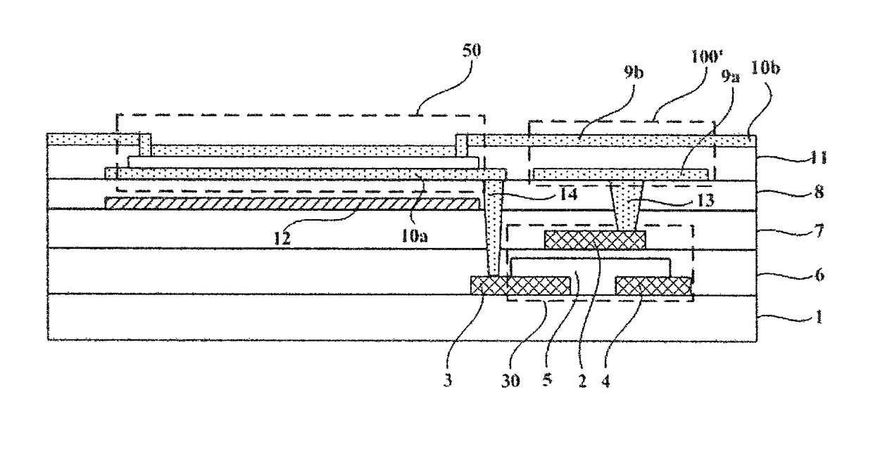
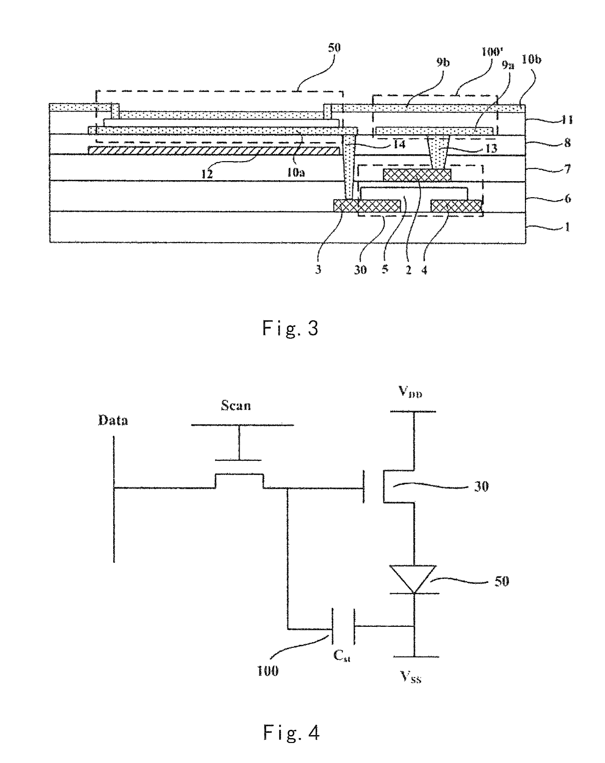
[0039]In order to improve the pixel aperture opening ratio of a display apparatus and thus to improve the display quality, an embodiment of the present invention provides an active matrix organic light-emitting diode (abbreviated as AMOLED below) array substrate and a method for producing the same and a display apparatus. In the technical solution of the array substrate of the present invention, the top plate of the storage capacitor may be spaced apart from the bottom plate of the storage capacitor by the pixel definition layer. The part of pixel definition layer located between the top plate and the bottom plate of the storage capacitor is used as a dielectric layer of the storage capacitor. As the pixel definition layer has occupied a certain light emitting area in itself, the top and bottom plates of the storage capacitor provided on both sides of the pixel definition layer will not need to occupy extra light emitting area. Thus, the area of opaque gate electrode and source elec...


PUM


Abstract

The present disclosure provides an active matrix organic light-emitting diode array substrate comprising: a substrate; a plurality of pixel units located on the substrate and arranged in an array, each of the plurality of pixel units comprising a thin film transistor, an organic light-emitting diode and a bottom plate of a storage capacitor; a pixel definition layer spacing apart two adjacent pixel units from each other; and a top plate of the storage capacitor provided on the pixel definition layer, the top plate of the storage capacitor being spaced apart from the bottom plate of the storage capacitor by the pixel definition layer. The bottom plate is arranged above a gate electrode of the thin film transistor and electrically connected to the gate electrode of the thin film transistor.

Description

[0001]This application is a Section 371 National State Application of International Application No. PCT / CN2014 / 085411, filed 28 Aug. 2014, entitled “AMOLED ARRAY SUBSTRATE, PRODUCING METHOD THEREOF AND DISPLAY APPARATUS, which has not yet published, which claims priority to Chinese Patent Application No. 201410183223.6 filed on Apr. 30, 2014 with the State Intellectual Property Office of China, the contents of which are incorporated herein by reference in their entirety.BACKGROUND OF THE INVENTION[0002]Field of the Invention[0003]The present disclosure relates to the technical field of display, in particular, relates to an AMOLED array substrate, a producing method thereof and a display apparatus.[0004]Description of the Related Art[0005]OLED (organic light-emitting diode abbreviated as OLED) may be classified into two categories, that is, a passive matrix (abbreviated as PM) PMOLED and an active matrix (abbreviated as AM) AMOLED, depending on its driving modes. The AMOLED may be cl...

Claims


Application Information

Patent Timeline
Patent Type & Authority Patents(United States)
IPC IPC(8): H01L27/32
CPCH01L27/3265H01L27/3246H01L27/3276H01L27/3262H01L2227/323H10K59/122H10K59/1216H10K59/131H10K59/1201H10K59/1213
Inventor WANG, JILIANGLI, ZHONGJUN
Owner BOE TECH GRP CO LTD
Why Eureka
Try Eureka