Optical module

a technology of optical modules and optical signals, applied in the field of optical modules, can solve the problems of lowering the waveform quality of optical signals, complicated soldering, affecting the processing cost and yield of optical modules, etc., and achieves the effect of not increasing a cost, and excellent high-frequency characteristics

Active Publication Date: 2017-06-27
LUMENTUM JAPAN INC
View PDF4 Cites 3 Cited by
  • Summary
  • Abstract
  • Description
  • Claims
  • Application Information

AI Technical Summary

Benefits of technology

[0009]It is an object of the present invention to provide a mode of an inexpensive optical module that is capable of transmitting or receiving high-speed optical signals, is excellent in high-frequency characteristics, and does not increase a cost.
[0010](1) An optical module according to one embodiment of the present invention includes: an optical subassembly configured to convert at least one of an optical signal or an electrical signal into another one of the optical signal and the electrical signal; a wiring substrate that has a wiring pattern including a connecting portion and is arranged on the optical subassembly so as to be electrically connected thereto; and a flexible insulating layer formed between the optical subassembly and the wiring substrate, the optical subassembly including: a conductive stem that has a surface opposed to the wiring substrate, the conductive stem being shaped so that the surface has a through hole opened therein and being connected to a reference potential; and a signal lead for transmitting a signal, the signal lead passing through the through hole while being electrically insulated from the conductive stem, the signal lead passing through the flexible insulating layer to be joined to the connecting portion, the flexible insulating layer being in contact with the connecting portion, the signal lead, and the surface of the conductive stem. According to the present invention, a space between the connecting portion and the signal lead, a space between the connecting portion and the surface of the stem, and a space between the signal lead and the surface of the stem are filled with the flexible insulating layer, and hence neither a space with only air nor a vacuumed space is formed therein. Thus, parasitic inductance of the signal lead can be reduced.

Problems solved by technology

At locations in the transmission line at which there are mismatches in the characteristic impedance, reflection waves of the electrical signals are generated to interfere with original modulated electrical signals, resulting in lowered waveform quality of optical signals.
However, if a unique flexible printed board connection method, e.g., the one proposed in Japanese Patent Application Laid-open No. 2009-302438, is employed for suppressing impedance mismatches, soldering is complicated, thereby influencing processing costs and yields of optical modules.
As a result, the optical modules may not be stably manufactured and supplied.

Method used


Image

  • Optical module
  • Optical module
  • Optical module

Examples


first embodiment

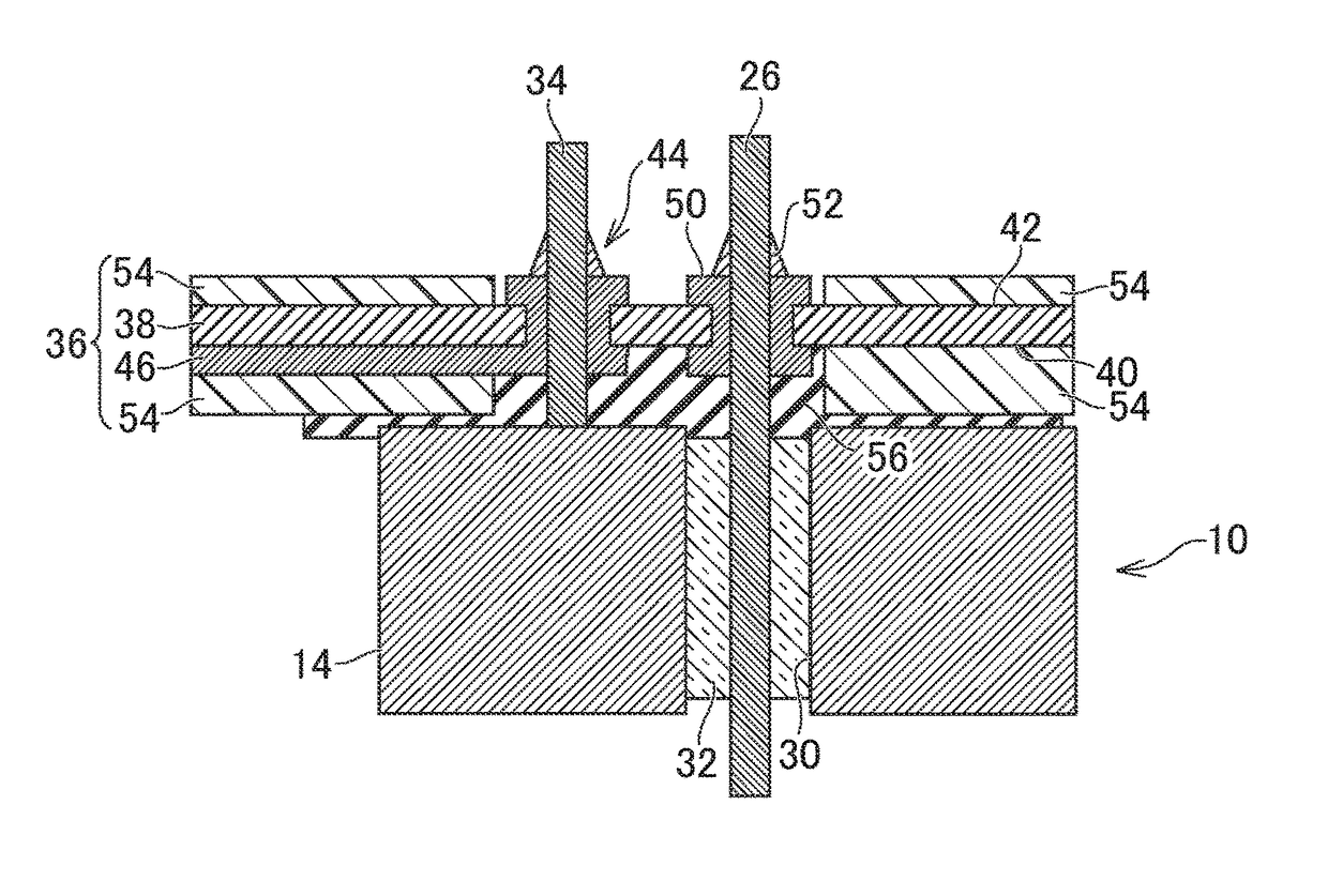
[0033]FIG. 1 is a sectional view for schematically illustrating an optical module according to a first embodiment of the present invention. The optical module includes an optical subassembly 10 configured to convert at least one of an optical signal or an electrical signal into the other. Examples of the optical subassembly 10 include an optical transmitter module (transmitter optical subassembly; TOSA) that includes a light emitting element, e.g., a semiconductor laser 12, and is configured to convert an electrical signal into an optical signal and transmit the optical signal, an optical receiver module (receiver optical subassembly; ROSA) that includes a light receiving element represented by a photodiode and is configured to convert a received optical signal into an electrical signal, and a bidirectional optical subassembly (BOSA) having both the functions of those optical subassemblies.

[0034]The invention of the subject application can be applied to any of the above-mentioned op...

second embodiment

[0047]FIG. 4 is a sectional view for illustrating the details of an optical module according to a second embodiment of the present invention. In this embodiment, an insulating material 232 is filled so that a projecting portion 258 maybe formed that protrudes from a surface of a stem 214. The projecting portion 258 is formed by the insulating material 232 creeping along a signal lead 226 by the surface tension, due to variations between lots. In such a case, a flexible insulating layer 256 has a recessed portion 260 in contact with the projecting portion 258. That is, the flexible insulating layer 256 absorbs the projecting portion 258 of the insulating material 232, and hence a wiring substrate 236 is mounted on the stem 214 without forming any air gap therebetween. It is therefore not necessary to consider how much the insulating material 232 creeps up, when designing the stem 214, thereby providing an effect of reducing the price of the stem 214. The description made in the first...

third embodiment

[0048]FIG. 5 is a sectional view for illustrating the details of an optical module according to a third embodiment of the present invention. In this embodiment, a protective film 354 formed on a first surface 340 overlaps a region other than a stem 314. The protective film 354 is not formed between the stem 314 and a wiring substrate 336, and hence a wiring pattern 344 and a signal lead 326 can be joined to each other at a position close to the stem 314. Impedance mismatch can therefore be reduced compared to the first embodiment, and hence excellent high-frequency characteristics can be expected. The description made in the first embodiment is applied to the third embodiment about the remaining structures.


PUM


Abstract

An optical module includes: a wiring substrate that has a wiring pattern including a connecting portion and is arranged on an optical subassembly so as to be electrically connected thereto; and a flexible insulating layer formed between the optical subassembly and the wiring substrate. The optical subassembly includes: a conductive stem that has a surface opposed to the wiring substrate, the conductive stem being shaped so that the surface has a through hole opened therein and being connected to a reference potential; and a signal lead for transmitting a signal, the signal lead passing through the through hole while being electrically insulated from the conductive stem. The signal lead passes through the flexible insulating layer to be joined to the connecting portion. The flexible insulating layer is in contact with the connecting portion, the signal lead, and the surface of the conductive stem.

Description

CROSS-REFERENCE TO RELATED APPLICATION[0001]The present application claims priority from Japanese application JP2015-118924 filed on Jun. 12, 2015, the content of which is hereby incorporated by reference into this application.BACKGROUND OF THE INVENTION[0002]1. Field of the Invention[0003]The present invention relates to an optical module.[0004]2. Description of the Related Art[0005]A CAN-type optical module used in optical communication generally includes an electrically-grounded stem and a lead terminal that passes through the stem and is insulated from the stem. The stem and a cap mounted to the stem form a housing for accommodating an optical semiconductor device. The lead terminal and the stem form a coaxial line. One end portion of the lead terminal is connected to the optical semiconductor device. Another end portion of the lead terminal is connected to a drive device configured to output a modulated electrical signal, via a wiring substrate, e.g., an FPC having a signal lin...

Claims


Application Information

Patent Timeline
Patent Type & Authority Patents(United States)
IPC IPC(8): H01S5/022H01S5/062H01S5/024
CPCH01S5/02212H01S5/02276H01S5/06226H01S5/02288H01S5/02469H01S5/02253H01S5/02345H05K999/99
Inventor NOGUCHI, DAISUKEKOMATSU, KAZUHIRO
Owner LUMENTUM JAPAN INC
Why Eureka
Try Eureka