Optical semiconductor device with flexible substrate

a technology of optical semiconductor and flexible substrate, which is applied in the direction of semiconductor lasers, cross-talk/noise/interference reduction, etc., can solve the problems of prone to mismatch in characteristic impedance, no longer applicable to optical transceivers, and the withdrawal of conventional optical semiconductor devices. , to achieve the effect of reducing the high-frequency signal

Active Publication Date: 2012-01-31
LUMENTUM JAPAN INC
View PDF6 Cites 5 Cited by
  • Summary
  • Abstract
  • Description
  • Claims
  • Application Information

AI Technical Summary

Benefits of technology

[0008]It is therefore an object of the invention to provide an optical semiconductor device using a CAN type optical package, wherein a flexible substrate, and a CAN type optical package are solidly joined with each other, the optical semiconductor device being excellent in high-frequency characteristics because reflection of a high frequency signal, occurring to joints, is reduced while maintaining its reliability as a product.
[0009]The present invention relates to a structure for connecting a CAN type optical package provided with a plurality of lead pins extending from a stem, arranged along a vertical direction, to a flexible substrate on which a metal pattern is patterned in order to fixedly attach the lead pins to the flexible substrate, ensuring electrical continuity therebetween.
[0010]The flexible substrate is bent at its spot corresponding to an end of a signal metal pattern on the flexible substrate to the extent that a substantially right angle is formed. And at least a signal lead pin, among the lead pins attached to the stem, is fixedly attached to a signal electrical pattern on the flexible substrate so as to be in a posture substantially horizontal with each other, ensuring electrical continuity therebetween.
[0013]With the present invention, part of the lead pins attached to the stem are fixedly attached to the respective electrical patterns, in such a state as penetrated through respective holes provided in the flexible substrate, so that the flexible substrate, and the CAN type optical package are solidly joined with each other. Meanwhile, because the lead pin for use in transmission of a high-frequency signal, and the metal pattern on the top of the flexible substrate are connected to each other in a posture substantially horizontal to each other, the present invention has an advantage in that reflection of the high-frequency signal is reduced.

Problems solved by technology

In recent years, however, a transmission speed in excess of 10 Gbps, that is, a transmission speed on the order of 25 Gbps, or 40 Gbps has come to be required of an optical transceiver, so that drawbacks of the conventional optical semiconductor device have since become so pronounced that the same is no longer applicable to the optical transceiver.
A mismatch in characteristic impedance is prone to occur to each spot where an optical transmission line is abruptly bent, thereby inducing reflection of a high frequency signal.
Since the reflection of the high frequency signal will not only induce deterioration in transmission waveform but also cause the high-frequency signal to be radiated as a noise inside the box of the optical transceiver to thereby induce an erroneous operation of the optical transceiver.

Method used


Image

  • Optical semiconductor device with flexible substrate
  • Optical semiconductor device with flexible substrate
  • Optical semiconductor device with flexible substrate

Examples


first embodiment

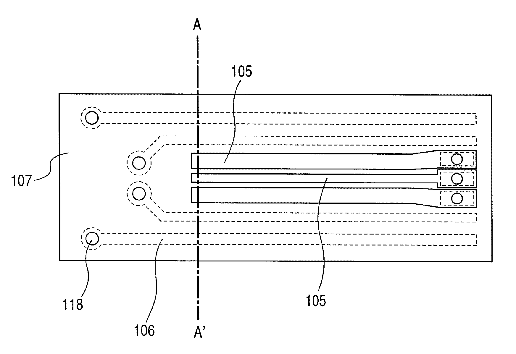
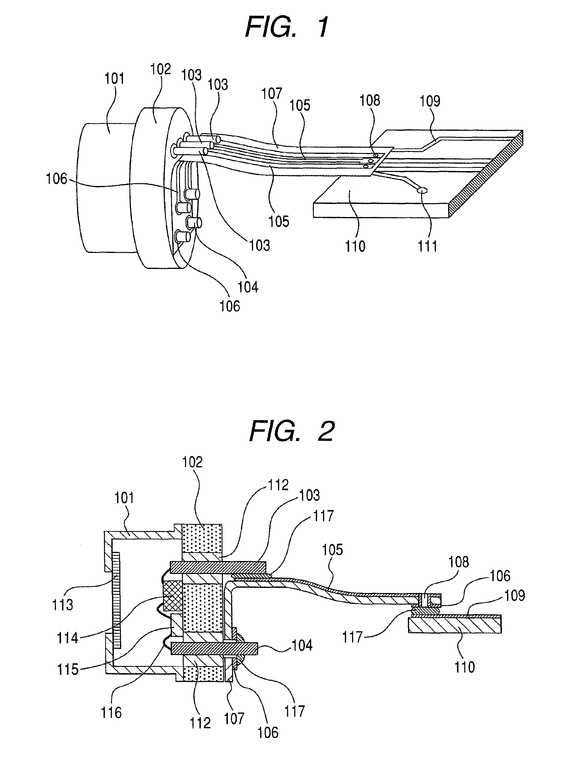
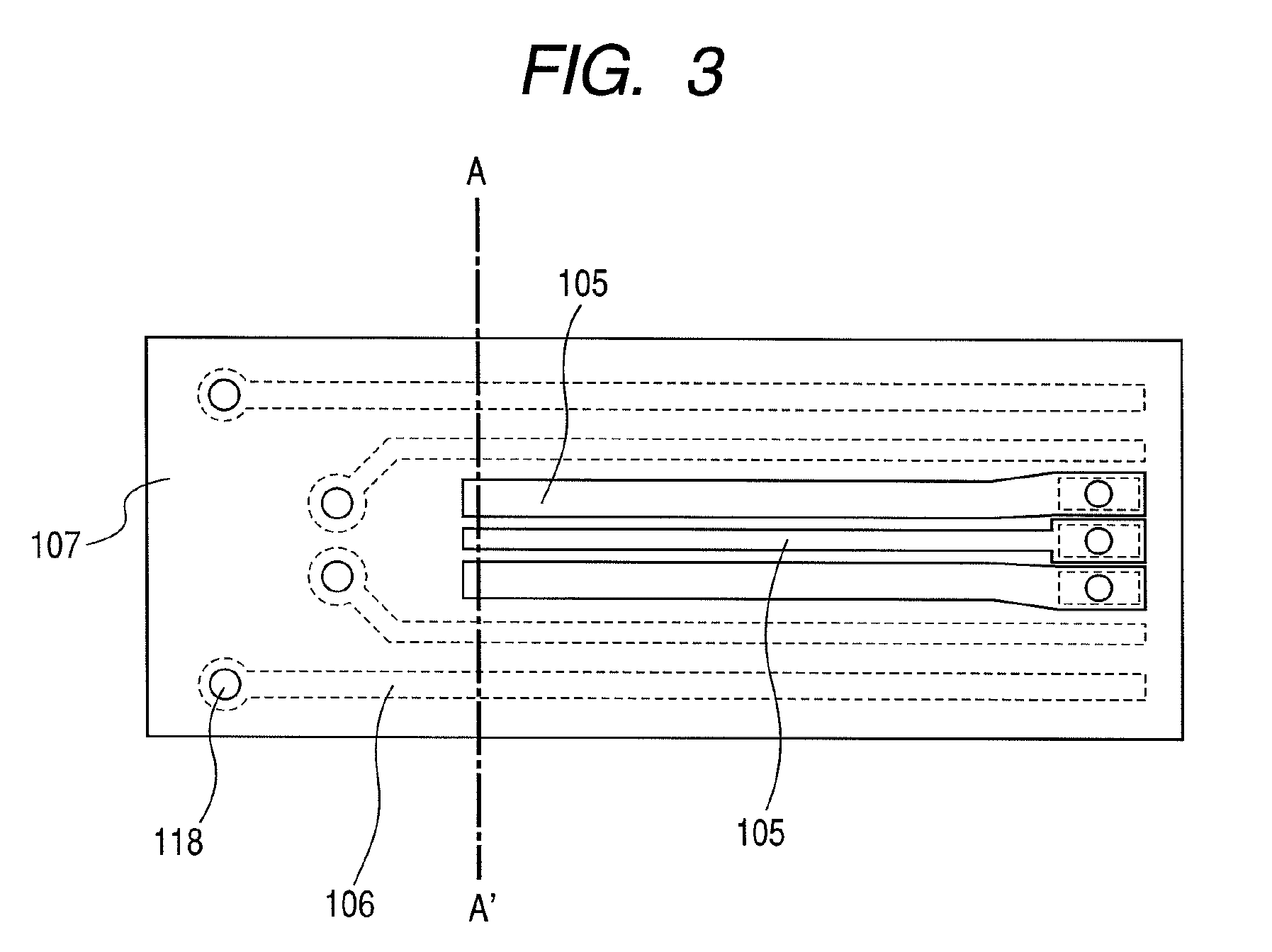
[0043]FIG. 1 is a perspective view schematically showing a first embodiment of an optical semiconductor device according to the invention, and a printed wiring board 110. The optical semiconductor device, and the printed wiring board 110 are components constituting an optical transceiver. FIG. 2 is a sectional view of the optical semiconductor device in FIG. 1, and FIG. 3 is a top view of a flexile substrate 107 only.

[0044]As shown in FIGS. 1 and 2, with a CAN type optical package, an optical element 115 is hermetically sealed with a lid 101 provided with a stem 102 and a window 113. An electronic element 114, and an optical element 115 are mounted on the stem 102, and wiring 116 is connected to respective spots where electrical connection is required, including first lead pins 103 and second lead pins 104, respectively. An insulator 112 is interposed between the stem 102 and each of the first lead pins 103 as well as each of the second lead pins 104. However, if a part of the lead ...

second embodiment

[0051]FIG. 4 is a top view of a flexile substrate 107 of an optical semiconductor device according to a second embodiment of the invention. The optical semiconductor device has an advantage in that the flexile substrate 107 is bent at a crease along line A-A′ in the figure, but the flexile substrate 107 can be bent with greater ease because the same is provided with a first notch 201 and a second hole 202. FIG. 5 is a sectional view of the flexile substrate 107, taken on line B-B′ of FIG. 4, and FIG. 6 is a sectional view of the flexile substrate 107, taken on line C-C′ of FIG. 4. With the flexile substrate 107, first metal patterns 105, and second metal patterns 106 are usually patterned on a base film 204, a resin layer 203 protecting the first metal patterns 105, and the second metal patterns 106, respectively. The base film 204, and the resin layer 203 each are composed of an organic matter such as resin including polyimide, and so forth. Further, a through-hole 108 with an inne...

third embodiment

[0052]FIG. 7 is a top view of a flexile substrate 107 of an optical semiconductor device according to a third embodiment of the invention. A metal pattern 301 for power supply or grounding, large in width, is patterned on the rear surface of the flexile substrate 107. Respective ends of first metal patterns 105, and an end of a metal pattern 301 for power supply or grounding are positioned in the vicinity of a crease along line A-A′ in the figure. A constituent material of the flexile substrate 107 is generally softer than that of the metal patterns. For this reason, if the end of such a metal pattern large in width is positioned in the vicinity of the crease along line A-A′, the flexile substrate 107 has an advantage in that it can be bent with greater ease.


PUM


Abstract

A metal pattern for a high frequency signal is patterned on a flexile substrate, and the flexile substrate is bent in such a way as to form a substantially right angle at a spot corresponding to an end of the metal pattern for the signal. And an end of the metal pattern is fixedly attached to a lead pin for signaling, attached to a stem, for electrical continuity, so as to be in a posture horizontal with each other. Meanwhile, a part of the lead pins attached to the stem, being in such a state as penetrated through respective holes provided in the flexible substrate, is fixedly attached to a part of metal patterns provided on the flexible substrate so as to ensure electrical continuity therebetween.

Description

CLAIM OF PRIORITY[0001]The present application claims priority from Japanese patent application JP 2008-157602, filed on Jun. 17, 2008, the content of which is hereby incorporated by reference into this application.FIELD OF THE INVENTION[0002]The invention relates to an optical semiconductor device encased in an optical transceiver that is used by taking advantage of an optical communication technology, and in particular, to an optical semiconductor device wherein a CAN type optical package, and a flexible substrate are joined with each other.BACKGROUND OF THE INVENTION[0003]In optical communication, an important role is played by an optical transceiver for transmitting and receiving an optical signal, and an optical fiber serving as a medium for transmission of the optical signal, respectively. An optical semiconductor device for converting an electric signal into an optical signal, and vice versa, and a printed wiring board with electronic elements for control, electrical connecto...

Claims


Application Information

Patent Timeline
Patent Type & Authority Patents(United States)
IPC IPC(8): H01L31/12
CPCH01L31/0203H01S5/02212H05K1/028H05K1/147H05K1/189H01L2224/48091H01L2924/01078H01L2924/01079H01L2924/3011H01S5/06226H05K1/0219H05K3/28H05K3/3421H05K3/3447H05K2201/0305H05K2201/09727H05K2201/10659H01L2924/00014H05K2201/10121
Inventor BAN, TAKUMASASADA, MICHIHIDEOKAYASU, MASANOBU
Owner LUMENTUM JAPAN INC
Why Eureka
Try Eureka