Dummy gate technology to avoid shorting circuit

a dummy gate and shorting circuit technology, applied in the direction of semiconductor devices, electrical apparatus, transistors, etc., can solve the problems of vsub>cc /sub>contacts, shorting through the dummy gate line of the edge cell, and contact ss /sub>contacts,

Active Publication Date: 2017-07-04
UNITED MICROELECTRONICS CORP
View PDF6 Cites 10 Cited by
  • Summary
  • Abstract
  • Description
  • Claims
  • Application Information

AI Technical Summary

Problems solved by technology

It was found that in the neighboring bit cell, various metal contacts, including bit line metal contacts, VSS contacts, VCC contacts, etc., which are positioned next to a dummy gate line of the edge cell have the risk of shorting through the dummy gate line of the edge cell,

Method used


Image

  • Dummy gate technology to avoid shorting circuit
  • Dummy gate technology to avoid shorting circuit
  • Dummy gate technology to avoid shorting circuit

Examples


Embodiment Construction

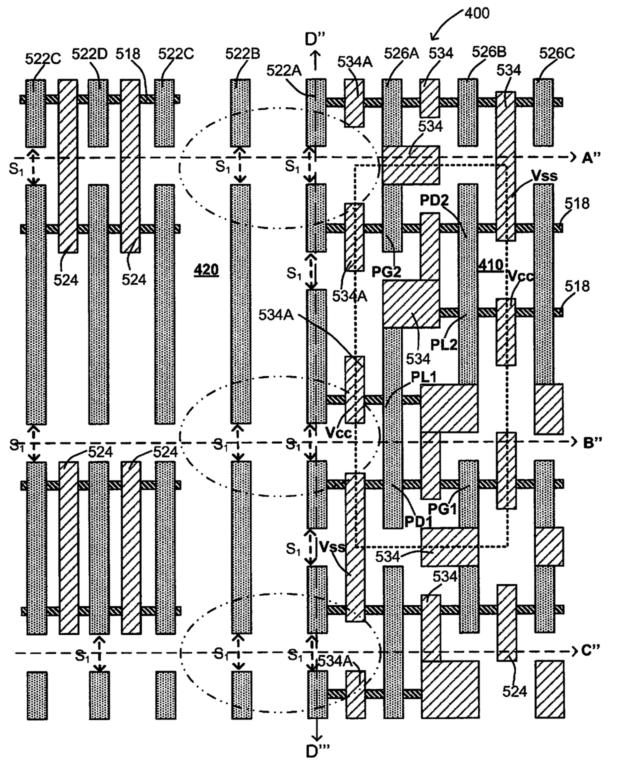
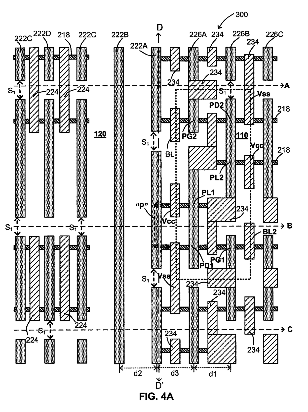
[0045]Embodiments of this invention provide a novel static random access memory (SRAM) comprising fin field-effect transistor (FinFET) structures to prevent electrical short to the dummy gate of an edge cell between a high VCC supply voltage of a metal contact disposed in an bit cell to a low VSS voltage of a nearby metal contact disposed in the same bit cell. In addition, the corresponding design layouts and a process of fabricating such improved SRAM (FinFETs) devices according to the improved device design layout for the corresponding edge cells and bit cells are presented.

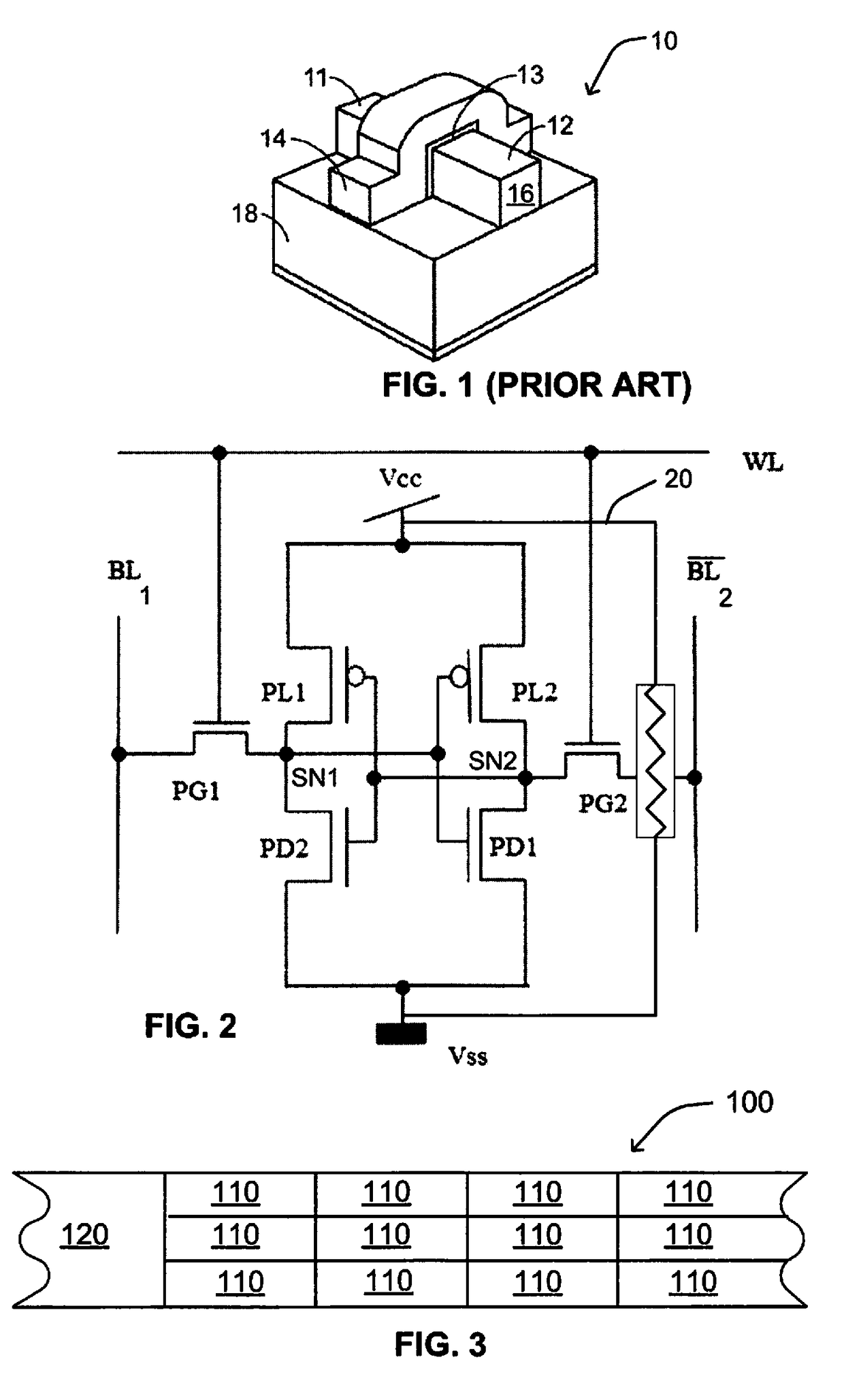
[0046]FIG. 2 is a circuit diagram of a static random access memory (SRAM) cell with 6 FinFET transistors (6T). The SRAM cell includes pass-gate transistors PG1 and PG2, pull-up transistors PL1 and PL2, and pull-down transistors PD1 and PD2. The gates of pass-gate transistors PG1 and PG2 are controlled by word-line (WL) that determines whether the current SRAM cell is selected or not. The storage portion of the ...


PUM


Abstract

Semiconductor devices and method of manufacturing such semiconductor devices are provided for improved FinFET memory cells to avoid electric short often happened between metal contacts of a bit cell, where the meal contacts are positioned next to a dummy gate of a neighboring dummy edge cell. In one embodiment, during the patterning of a gate layer on a substrate surface, an improved gate slot pattern is used to extend the lengths of one or more gate slots adjacent bit lines so as to pattern and sectionalize a dummy gate line disposed next to metal contacts of an active memory cell. In another embodiment, during the patterning of gate lines, the distances between one or more dummy gates lines disposed adjacent an active memory cell are adjusted such that their locations within dummy edge cells are shifted in position to be away from metal contacts of the active memory cell.

Description

BACKGROUND OF THE INVENTION[0001]Field of the Invention[0002]Embodiments of the invention relate to static random access memory (SRAM) to be used for storage on integrated circuit devices, and more particularly to advanced SRAM cells using one or more fin field-effect transistor (FinFET) structures. The present invention also relates to the design layout and manufacturing process for fabricating SRAM cells with such fin field-effect transistor structures.[0003]Description of the Related Art[0004]Modern digital data processors generally use several different types of memory devices to answer different performance and functional requirements. Dynamic memories generally store data as charge in a capacitor to allow much faster access, and can be selectively addressed for storing smaller amounts of data each time. However, dynamic memories must be periodically refreshed to compensate for charge that may leak from its capacitors, leading to undesirable longer access time.[0005]Static memo...

Claims


Application Information

Patent Timeline
Patent Type & Authority Patents(United States)
IPC IPC(8): H01L21/768H01L29/78H01L29/66H01L27/11H01L27/02
CPCH01L21/768H01L27/0207H01L27/1104H01L29/6681H01L29/7851H01L21/28H01L29/4232H10B10/00H10B10/12H01L21/845H01L27/1211H01L21/823821H01L27/0924H01L21/76816H01L21/76829H01L21/823871H01L29/66545
Inventor HUNG, CHING-WENHUANG, CHIH-SENTZOU, SHIH-FANGCHEN, YI-WEICHENG, YUNG-FENGHUANG, LI-PINGHUANG, CHUN-HSIENHUANG, CHIA-WEIKUO, YU-TSE
Owner UNITED MICROELECTRONICS CORP
Why Eureka
Try Eureka