Level shifter circuit with improved time response and control method thereof

a level shifter and time response technology, applied in logic circuits, pulse automatic control, pulse technique, etc., can solve the problems of slow operation, rc delay, and difficulty in increasing the gate-source voltage to a level of tens of volts

Active Publication Date: 2017-08-22
SILICON WORKS CO LTD
View PDF49 Cites 0 Cited by
  • Summary
  • Abstract
  • Description
  • Claims
  • Application Information

AI Technical Summary

Benefits of technology

[0030]Accordingly, the present invention has been made to solve the above problems occurring in the prior art, and an object of the present invention is to reduce RC delay and also improve time response characteristics in a level shifter circuit.
[0031]An object of the present invention is to provide a stable and fast high-voltage switching operation regardless of the characteristics of elements, such as the threshold voltages of transistors, etc., which constitute a circuit.
[0032]An object of the present invention is to deal with a wide voltage range in which a level shifter operates, to minimize operation-related limitations attributable to the characteristics of transistors, such as a breakdown voltage, etc., and to provide a high-voltage fast switching operation in various applications.

Problems solved by technology

It is known that they have a high drain-source breakdown voltage ranging from about 40 to about 50 V in common, but it is very difficult to increase their gate-source voltage to a level of tens of volts because the gate-source voltage is determined based on the thickness of the channel oxide of the transistors.
Although the circuit of FIG. 1 would operate according to the above-described method when observation is conducted over a long time interval, a problem arises in that the operation is actually delayed due to the parasitic capacitances Cr and Cp of the node 110 shown in FIG. 1.
However, in practice, the transition from OFF state to ON state is slowly performed with an RC delay due to time constant R1·(Cr+Cp).
To overcome this risk, inconvenience in circuit design arises in that reservoir capacitance corresponding to the node of VPHASE must be considerably high.
However, despite the improved circuit of FIG. 2, a problem still arises in that node 210 suffers from the delay of a time response attributable to an RC time constant.
Furthermore, another problem arises in that the improved circuit of FIG. 2 undergoes more difficulty in matching the threshold voltage characteristic of the transistors M1, M2 and M3 than the circuit of FIG. 1.
In the conventional art shown in FIG. 2, when the input control signal Φ transitions from an ON state to an OFF state (when Vx rises from a low voltage to a high voltage), the time required can be reduced, but this conventional art cannot provide a fundamental solution.
As a result, a problem arises in that the rising and falling characteristics of Vx are determined based on an RC time constant.
Furthermore, the conventional art shown in FIG. 2 is problematic in that since the lower limit of Vx is determined to be (VBOOT−VT,M3), the transistor M2 is turned off at the lower limit of Vx and thus can achieve its intended purpose only if the threshold voltage VT,M2 of the transistor M2 is considerably high.
For this purpose, the conventional art has a problem in that the condition of Equation 5 below must be satisfied:
In contrast, since the transistor M1 can achieve its intended purpose only if the transistor M1 is turned on at the lower limit of Vx, a problem arises in that the threshold voltage VT,M1 of the transistor M1 must satisfy Equation 6 below:
That is, the conventional art is problematic in that it cannot be a fundamental solution to an RC time delay and also it is very difficult to match the threshold voltage characteristics of transistors.

Method used


Image

  • Level shifter circuit with improved time response and control method thereof
  • Level shifter circuit with improved time response and control method thereof
  • Level shifter circuit with improved time response and control method thereof

Examples


Embodiment Construction

[0066]Embodiments of the present invention will be described in detail with reference to the accompanying drawings. In the following description of the present invention, detailed descriptions of related well-known components or functions that may unnecessarily make the gist of the present invention obscure will be omitted.

[0067]The prevent invention is not limited to the embodiments. Throughout the accompanying drawings, the same reference symbols are assigned to the same components.

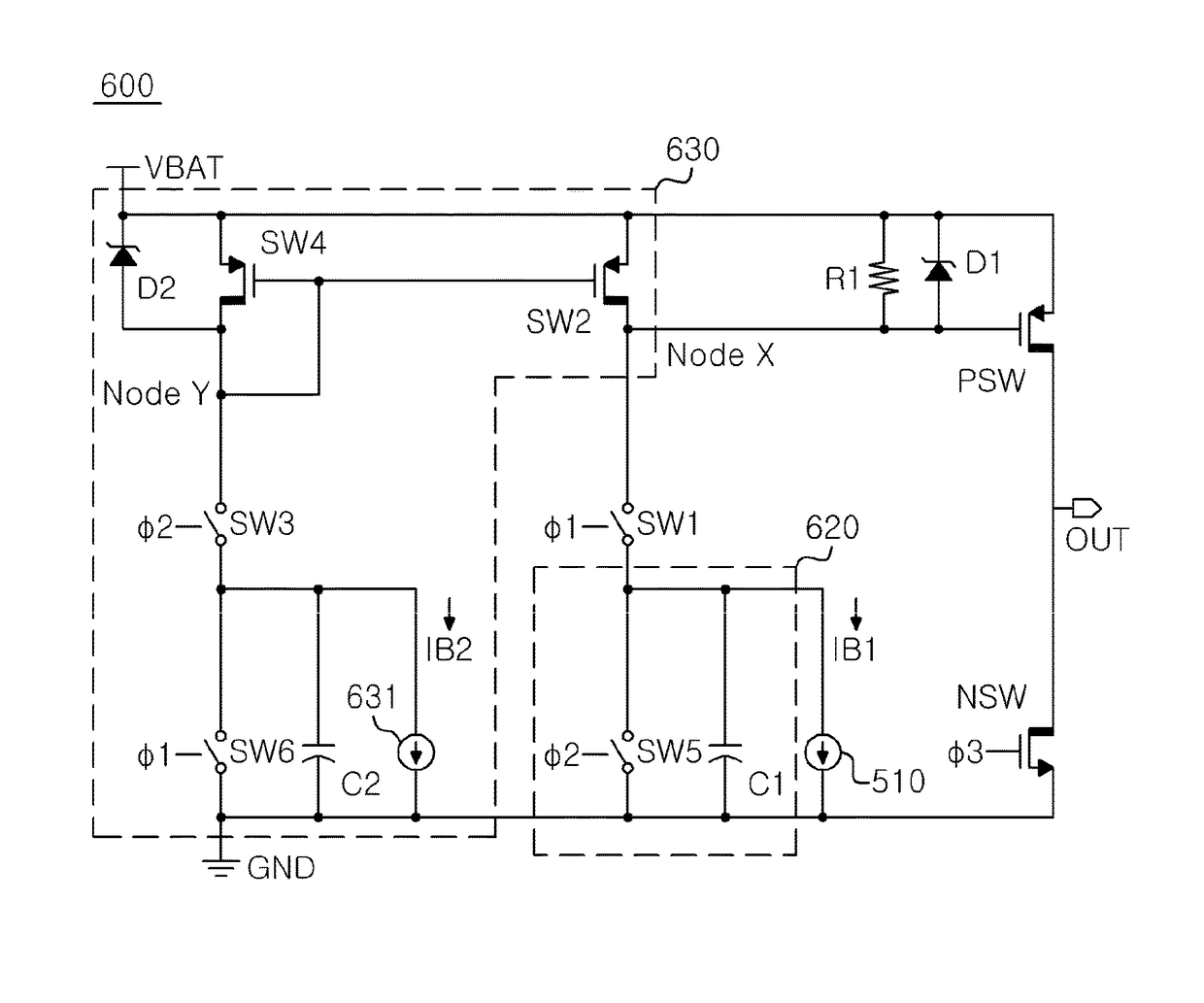
[0068]FIG. 3 is a diagram showing a portion 300 of a pass switch circuit according to an embodiment of the present invention.

[0069]Referring to FIG. 3, a first pass switch PSW configured to transfer the voltage level of an input node A to an output node B is shown. Although a P-type pass switch is shown as the first pass switch in FIG. 3, the idea of the present invention is not limited thereto. The first pass switch PSW is an element configured to transfer the voltage level of the input node A to the o...


PUM


Abstract

A level shifter circuit with improved time response and a control method thereof are disclosed herein. The level shifter circuit includes the output stage circuit of a level shifter and a booster circuit. The output stage circuit of the level shifter includes a first pass switch configured to transfer a voltage level of the first power supply of the level shifter to an output node, and a second pass switch connected between a second power supply and the first pass switch. The booster circuit accelerates the switching operation of the level shifter by accelerating a time response during the turning on or off operation of the first pass switch using charge sharing between a first capacitor and the parasitic capacitance of the control node of the first pass switch, which occurs via a first switch.

Description

CROSS-REFERENCE TO RELATED APPLICATION[0001]This application is a continuation of PCT / KR2015 / 000324 filed on Jan. 13, 2015, which application is incorporated herein by reference.TECHNICAL FIELD[0002]The present invention relates to a level shifter circuit for generating an output logic signal having a converted voltage level by converting the voltage level of an input logic signal, and more particularly to a level shifter circuit capable of improving time response characteristics, thereby enabling fast switching.BACKGROUND ART[0003]In electronic circuit applications supporting high-voltage switching operations, a circuit called a “level shifter” is used to transfer signals between circuit networks at different voltage levels. When a level shifter is combined with an inverter, the level shifter performs the function of converting a logic signal operating in the voltage range from 0 to V1 into an output signal operating in the voltage range from 0 to V2.[0004]Furthermore, a level shif...

Claims


Application Information

Patent Timeline
Patent Type & Authority Patents(United States)
IPC IPC(8): H03L5/00H03K19/017H03K19/00H03K19/0185
CPCH03K19/0013H03K19/01714H03K19/018521H03K19/018528
Inventor LEE, SEUNG JONGWOO, YOUNG JINCHO, HOO HYUN
Owner SILICON WORKS CO LTD
Why Eureka
Try Eureka