Printed circuit board package structure and manufacturing method thereof

a technology of printed circuit board and package structure, which is applied in the direction of printed element electric connection formation, association of printed circuit non-printed electric components, inductance, etc., can solve the problems of not being able to release pressure to possibly damage glass fibers and epoxy that covers the substrate, and achieve the effect of reducing the time spent on vertical movements (ascent and descent) of the cutting tool

Active Publication Date: 2017-08-22
TRIPOD TECHNOLOGY CORPORATION
View PDF7 Cites 9 Cited by
  • Summary
  • Abstract
  • Description
  • Claims
  • Application Information

AI Technical Summary

Benefits of technology

[0016]In the aforementioned embodiment, the cutting tool can be lowered into the substrate when forming the first ring-shaped recesses and the first grooves, and thereafter the cutting tool is allowed to cut and form the first ring-shaped recesses and the first grooves by moving horizontally. The cutting tool would not be lifted until the first ring-shaped recesses and the first grooves communicated with the first ring-shaped recesses are formed. Therefore, the time spent on vertical movements (ascent and descent) of the cutting tool can be reduced.

Problems solved by technology

As a result, pressure cannot be released to possibly damage the glass fibers and the epoxy that covers the substrate.

Method used


Image

  • Printed circuit board package structure and manufacturing method thereof
  • Printed circuit board package structure and manufacturing method thereof
  • Printed circuit board package structure and manufacturing method thereof

Examples


Embodiment Construction

[0034]In the following detailed description, for purposes of explanation, numerous specific details are set forth in order to provide a thorough understanding of the disclosed embodiments. It will be apparent, however, that one or more embodiments may be practiced without these specific details. In other instances, well-known structures and components are schematically depicted in order to simplify the drawings.

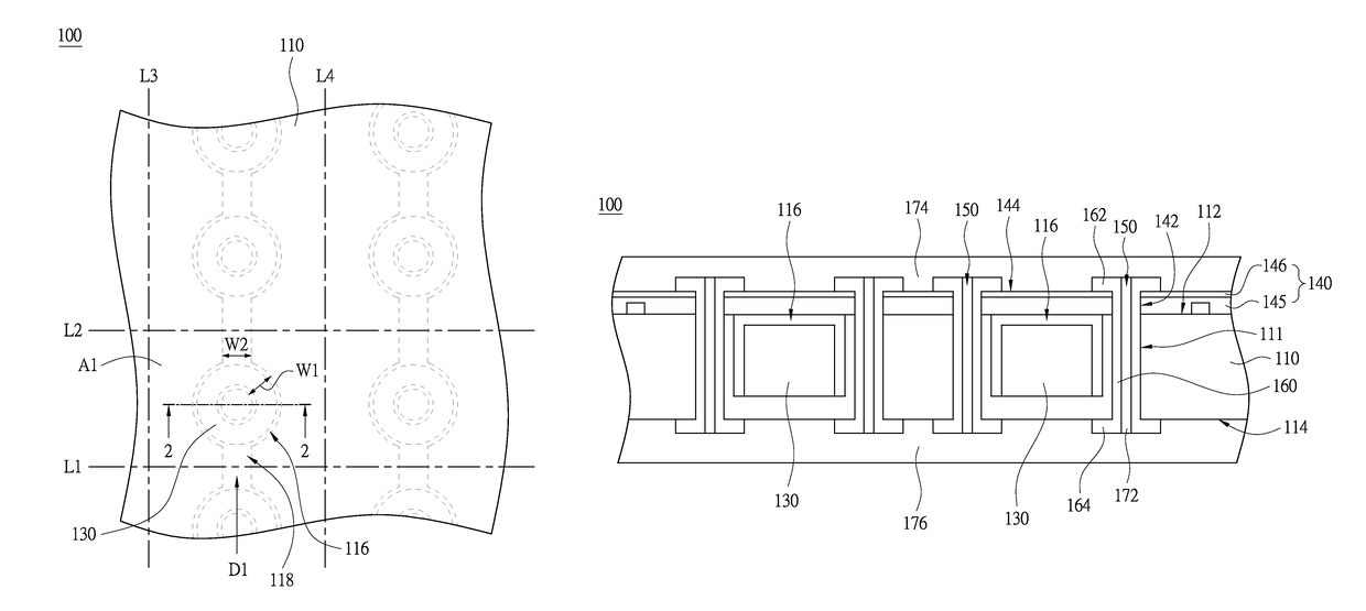
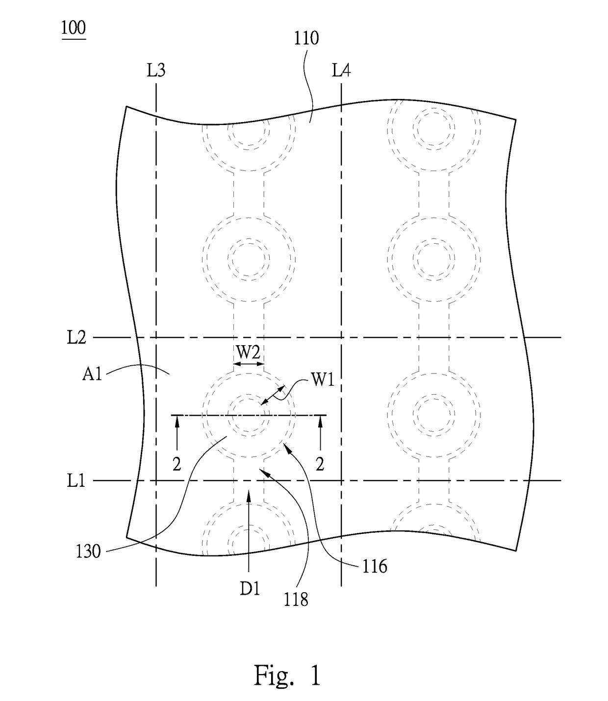
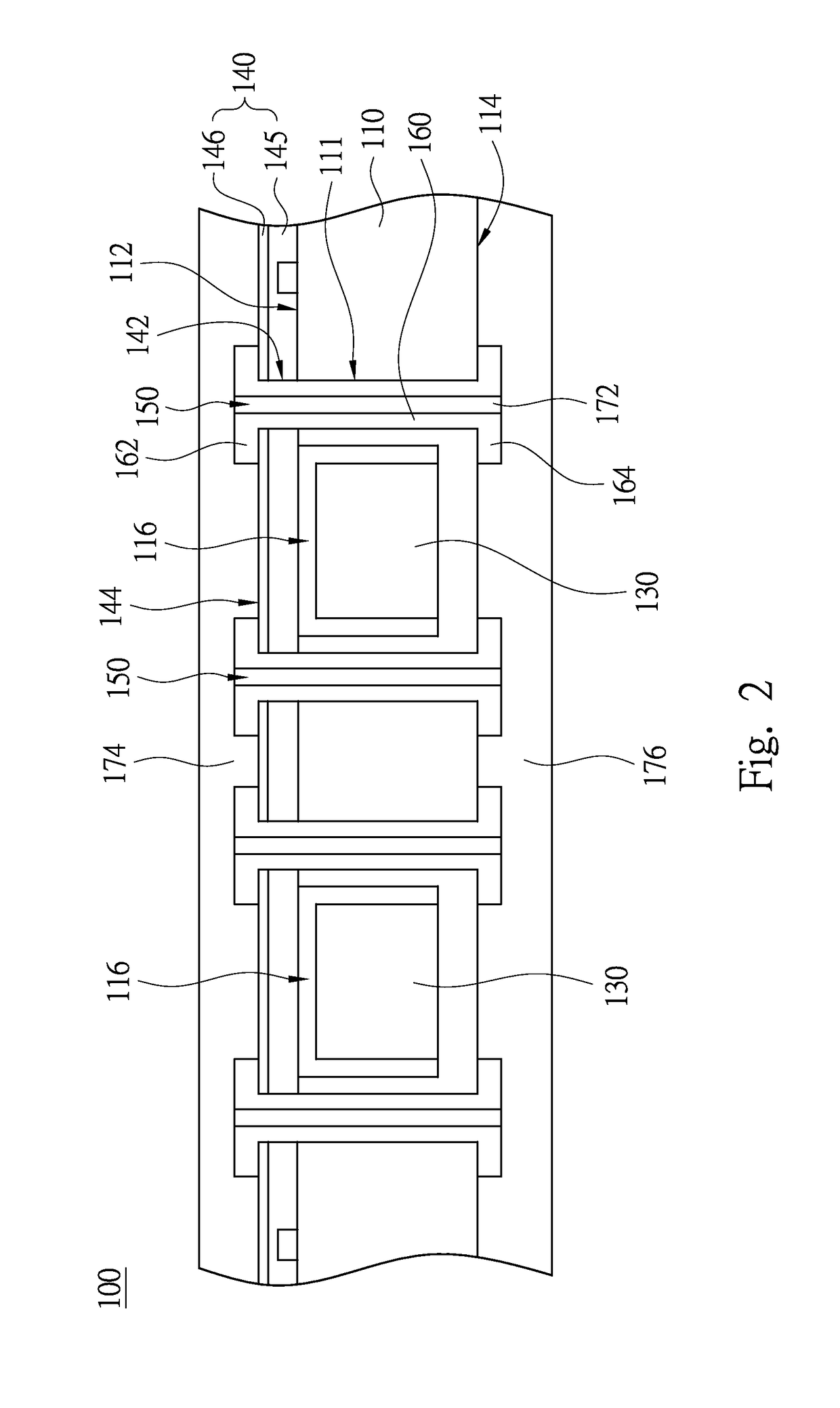
[0035]FIG. 1 is a top view of a printed circuit board package structure 100 according to one embodiment of this invention. FIG. 2 is a cross-sectional view of the printed circuit board package structure 100 taken along line 2-2 shown in FIG. 1. As shown in FIG. 1 and FIG. 2, the printed circuit board package structure 100 includes a substrate 110, a plurality of ring-shaped magnetic elements 130, a support layer 140, and a plurality of first conductive layers 160. The substrate 110 has a first surface 112 and a second surface 114 opposite to the first surface 112, a plurality...


PUM

PropertyMeasurementUnit
conductiveaaaaaaaaaa
diametersaaaaaaaaaa
distanceaaaaaaaaaa

Abstract

A printed circuit board package structure includes a substrate, plural ring-shaped magnetic elements, a support layer, and first conductive layers. The substrate has two opposite first and second surfaces, first ring-shaped recesses, and first grooves. Each of the first ring-shaped recesses is communicated with another first ring-shaped recess through at least one of the first grooves, and at least two of the first ring-shaped recesses are communicated with a side surface of the substrate through the first grooves to form at least two openings. The ring-shaped magnetic elements are respectively located in the first ring-shaped recesses. The support layer is located on the first surface, and covers the first ring-shaped recesses and the first grooves. The support layer and the substrate have through holes. The first conductive layers are respectively located on surfaces of support layer and substrate facing the through holes.

Description

RELATED APPLICATIONS[0001]This application claims priority to Taiwan Application Serial Number 102137722, filed on Oct. 18, 2013 and Taiwan application serial no. 103110521, filed on Mar. 20, 2014, which are herein incorporated by reference.BACKGROUND[0002]Field of Invention[0003]The present invention relates to a printed circuit board package structure and a manufacturing method thereof.[0004]Description of Related Art[0005]Generally speaking, in the manufacturing process of a printed circuit board, a specific element, such as a copper block for heat dissipation, a core, etc., needs to be placed into a preset accommodation recess of the printed circuit board. The core, being magnetic, can be used in a transformer structure or a power choke structure.[0006]In a conventional printed circuit board having a four-layered package structure, a copper clad laminate (CCL) is used as a substrate. When the printed circuit board is manufactured, a forming machine can be utilized to form a plur...

Claims


Application Information

Patent Timeline
Patent Type & Authority Patents(United States)
IPC IPC(8): H05K1/03H05K1/11H05K3/42H01F17/00H01F17/06H01F41/04H05K3/46H01F27/28H05K1/18H05K1/16H05K3/00H05K1/02
CPCH05K1/181H01F17/0006H01F17/06H01F27/2804H01F41/046H05K1/0366H05K1/115H05K3/427H05K3/4602H05K3/4697H05K1/0272H05K1/165H05K3/0044H05K3/0052H05K3/4655H05K2201/0187H05K2201/0275H05K2201/086H05K2201/09036H05K2201/1003H05K2203/1178Y10T29/302Y10T29/49165
Inventor HUANG, BO-SHIUNGYANG, WEI-HSIUNGSHIH, HAN-CHINGLIN, CHENG-FENG
Owner TRIPOD TECHNOLOGY CORPORATION
Why Eureka
Try Eureka