Fabrication method of a stack of electronic devices

a technology of electronic devices and fabrication methods, applied in the direction of basic electric elements, semiconductor/solid-state device manufacturing, electric devices, etc., can solve the problems of poor quality, closed oxide/oxide bonding interface, and state-of-the-art methods are not entirely satisfactory, and achieve good-quality direct bonding

Active Publication Date: 2017-10-03
COMMISSARIAT A LENERGIE ATOMIQUE ET AUX ENERGIES ALTERNATIVES
View PDF15 Cites 0 Cited by
  • Summary
  • Abstract
  • Description
  • Claims
  • Application Information

AI Technical Summary

Benefits of technology

[0017]to obtain a bonding interface with a good closing quality (resistant in particular to wet chemistry etching processes) due to the hydrophobic bonding of step c) by means of the first and second semiconductor layers, thereby circumventing the need for reinforcement thermal annealing of the bonding interface with a high thermal budget, i.e. an annealing temperature of about 1000-1200° C. and an anneal time of a few hours;
[0038]Such a step thus enables good-quality direct bonding to be obtained between the first and second semiconductor layers.

Problems solved by technology

Such a state-of-the-art method is not entirely satisfactory in so far as the closing of the oxide / oxide bonding interface, obtained after the hydrophilic bonding of step c), is generally of poor quality.
Such a partially open bonding interface is therefore liable to lead to extensive infiltration of the etching agents into the first dielectric layer possibly during step d), or more generally at a subsequent stage when the electronic device is formed from the active layer.
This infiltration then causes lift-off of the active layer, thereby resulting in a loss of active surface.
Lift-off of the active layer is furthermore liable to lead to a considerable defectivity when formation of the electronic device takes place.
Such a thermal budget is incompatible with most electronic devices which are liable to be impaired.

Method used


Image

  • Fabrication method of a stack of electronic devices
  • Fabrication method of a stack of electronic devices
  • Fabrication method of a stack of electronic devices

Examples


Embodiment Construction

[0047]For the different embodiments, the same reference numerals will be used for parts that are identical or which perform the same function, for the sake of simplification of the description. The technical characteristics described in the following for different embodiments are to be considered either alone or in any technically possible combination.

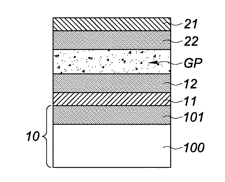
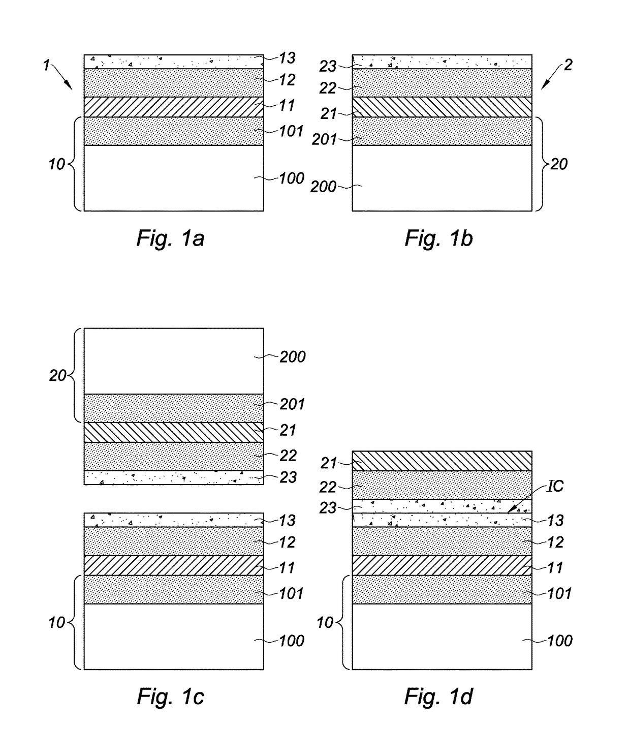
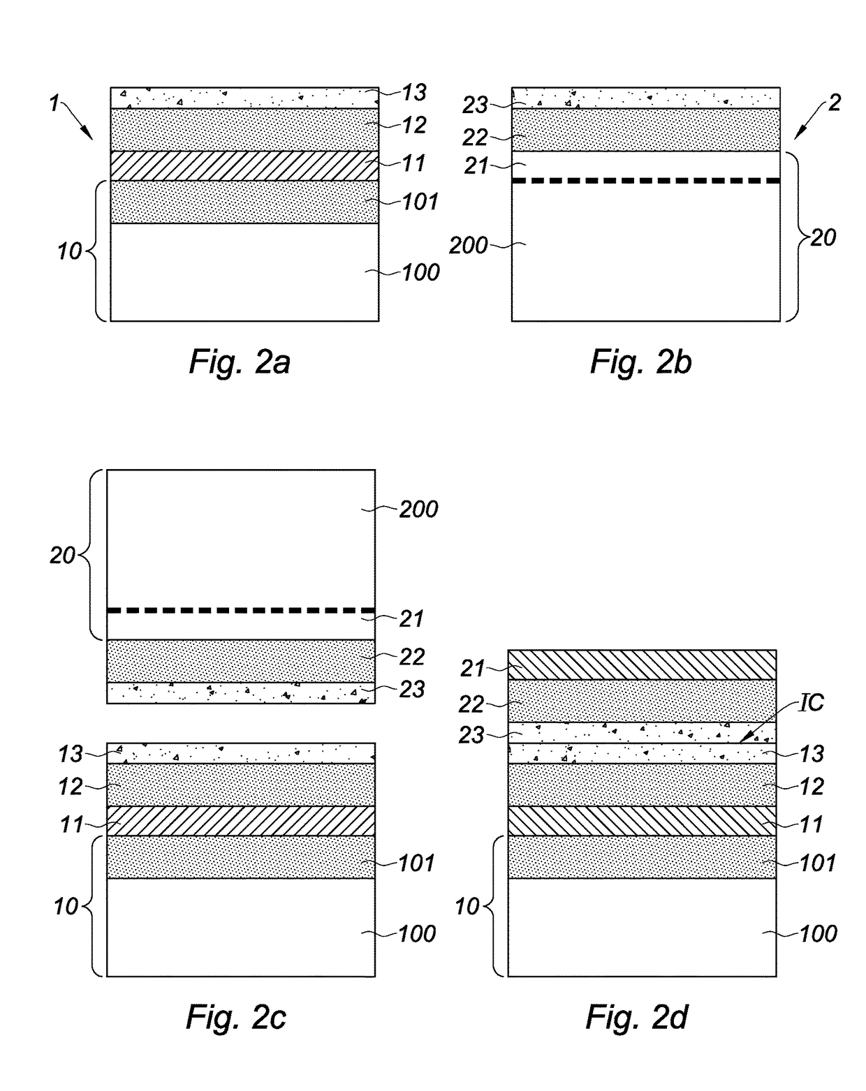
[0048]The method illustrated in FIGS. 1a to 1d, 2a to 2d, and 3a to 3e is a fabrication method of a stack of electronic devices 11, 21, comprising the following steps:[0049]a) providing a first structure 1 successively comprising a substrate 10, an electronic device 11, a dielectric layer 12, and a first semiconductor layer 13;[0050]b) providing a second structure 2 successively comprising a substrate 20, an active layer 21, a dielectric layer 22, and a second semiconductor layer 23, the active layer 21 being designed to form an electronic device;[0051]c) bonding the first and second structures 1, 2 by direct bonding between the first ...


PUM


Abstract

This method includes the following steps: a) providing a first structure successively including a substrate, an electronic device, a dielectric layer, and a first semiconductor layer; b) providing a second structure successively including a substrate, an active layer, a dielectric layer, and a second semiconductor layer, the active layer being designed to form an electronic device; c) bonding the first and second structures by direct bonding between the first and second semiconductor layers so as to form a bonding interface; d) removing the substrate of the second structure so as to expose the active layer; e) introducing dopants into the first and second semiconductor layers so as to form a ground plane.

Description

BACKGROUND OF THE INVENTION[0001]The present invention relates to a fabrication method of a stack of electronic devices. As non-restrictive examples, an electronic device can be a transistor, a memory, a micro electromechanical system (MEMS) etc. An envisaged application is 3D Very-Large-Scale Integration (VLSI) by means of the CoolCube™ technology in order to successively fabricate transistors, the top transistors being fabricated at low temperature (typically less than 500° C.).STATE OF THE ART[0002]A known method of the state of the art comprises the following steps:[0003]a) providing a first structure successively comprising a substrate, an electronic device, and a first dielectric layer;[0004]b) providing a second structure successively comprising a substrate, an active layer, and a second dielectric layer, the active layer being designed to form an electronic device;[0005]c) bonding the first and second structures by direct bonding between the first and second dielectric layer...

Claims


Application Information

Patent Timeline
Patent Type & Authority Patents(United States)
IPC IPC(8): H01L21/76H01L21/762H01L21/02
CPCH01L21/76251H01L21/02532H01L21/02592H01L21/02667H01L21/185H01L21/76254H01L21/8221
Inventor BATUDE, PERRINEBRUNET, LAURENTFENOUILLET-BERANGER, CLAIREFOURNEL, FRANK
Owner COMMISSARIAT A LENERGIE ATOMIQUE ET AUX ENERGIES ALTERNATIVES
Why Eureka
Try Eureka