Embedded antenna device for electronic communication device

a technology of electronic communication device and antenna device, which is applied in the direction of antenna, antenna earthing, antenna details, etc., can solve the problem of reducing portability

Inactive Publication Date: 2017-10-31
SAMSUNG ELECTRONICS CO LTD +1
View PDF11 Cites 0 Cited by
  • Summary
  • Abstract
  • Description
  • Claims
  • Application Information

AI Technical Summary

Benefits of technology

[0011]An aspect of the present invention is to address at least the above-mentioned problems and / or disadvantages and to provide at least the advantages described below. Accordingly, an aspect of the present invention is to provide a built-in antenna device for an electronic device for communication, realized to operate in a multiple band without increasing an installation effective space inside the electronic device.
[0013]Still another aspect of the present invention is to provide a built-in antenna device for an electronic device for communication, realized to be easily installed and simultaneously to contribute slimness of the electronic device.
[0016]An electronic device for communication according to the present invention has an effect of allowing the built-in antenna radiator to operate in at least one desired frequency band by allowing a transmission line to branch from a feeding line of an existing built-in antenna device and thus controlling reactance.

Problems solved by technology

In this case, the antenna becomes a most fragile portion that may be destroyed when the terminal drops down, and causes a problem of reducing portability.

Method used


Image

  • Embedded antenna device for electronic communication device
  • Embedded antenna device for electronic communication device
  • Embedded antenna device for electronic communication device

Examples


Embodiment Construction

[0029]A preferred embodiment of the present invention is described below in detail with reference to the accompanying drawings. However, descriptions of well-known functions and constructions are omitted since they may obscure the spirit of the present invention unnecessarily.

[0030]Though a portable terminal as an electronic device for communication is illustrated and described in describing the present invention, it is not limited thereto. For example, the present invention is applicable to an electronic device of various fields, used for communication even though it is not carried with.

[0031]Furthermore, in describing the present invention, a bar type terminal has been illustrated and an antenna device mounted therein has been described. However, a built-in antenna device according to the present invention may be mounted inside a terminal having various open types such as a folder type terminal, a slide type terminal, etc.

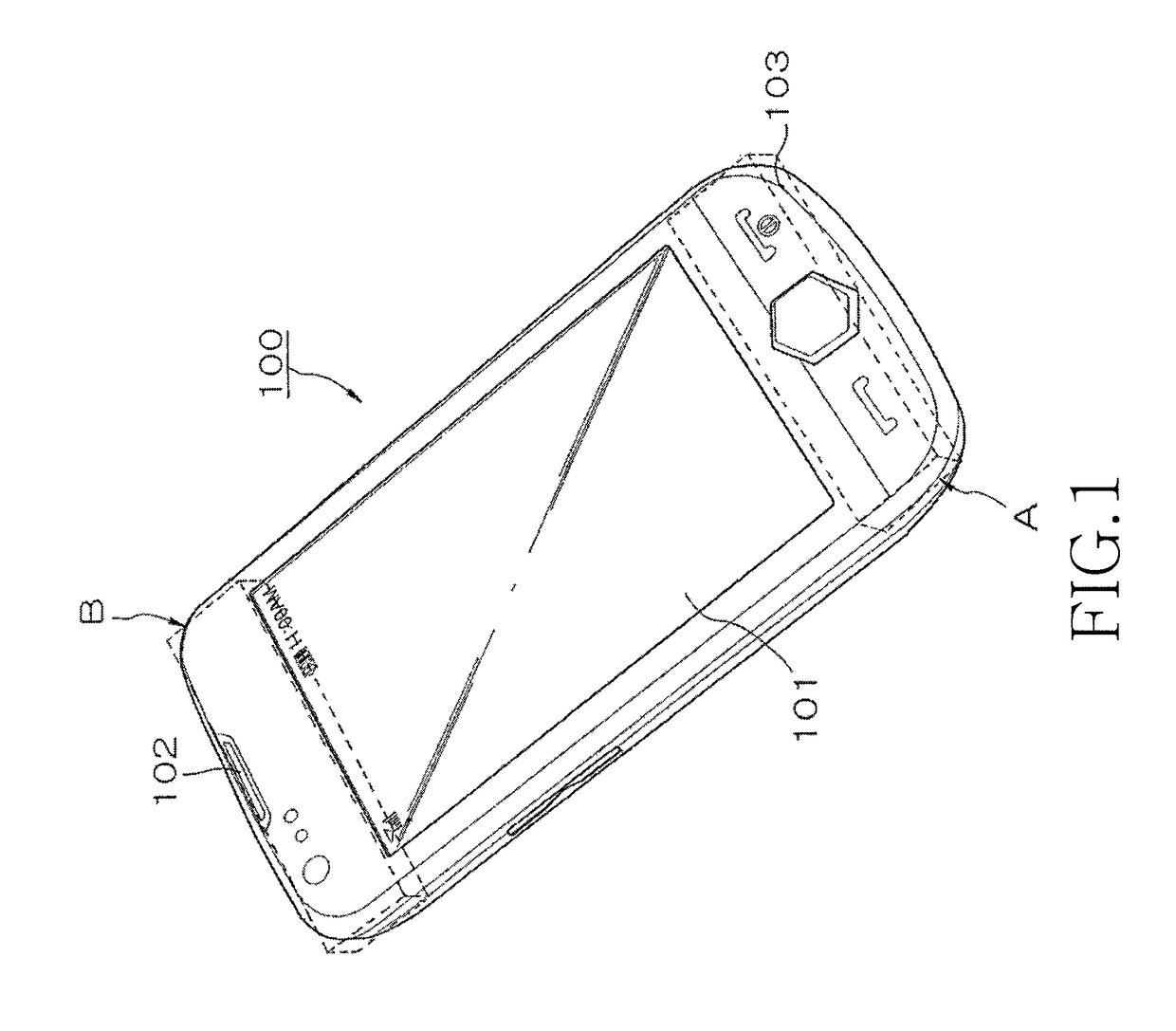
[0032]FIG. 1 is a perspective view illustrating a portable ...


PUM


Abstract

A built-in antenna device for an electronic device for communication is provided. The antenna device includes a substrate, an antenna radiator, and a transmission line. The substrate includes a grounding region and a non-grounding region. The antenna radiator is disposed in the non-grounding region of the substrate and fed from a feeding portion provided to the substrate. The transmission line branches from the antenna radiator and is disposed in vicinity of the grounding region to have a predetermined length and a predetermined width. The antenna device controls reactance by coupling the transmission line with the grounding region to allow the antenna radiator to operate in at least one desired band.

Description

BACKGROUND OF THE INVENTION[0001]1. Field of the Invention[0002]The present invention relates to a built-in antenna device. More particularly, the present invention relates to a built-in antenna device for an electronic device for communication, realized for contributing to a slim profile of the device and simultaneously securing a wideband.[0003]2. Description of the Related Art[0004]Recently, an electronic device for communication, having various functions and designs emerges. A portable terminal is a representative device of these electronic devices. The portable terminal becomes lightweight and miniaturized in a slim profile and simultaneously diversity of its function stands out even more. Therefore, the portable terminal places an emphasis on reduction of its volume while maintaining or improving its functions in order to meet this desire of a consumer.[0005]Particularly, a folder type terminal and a slide type terminal among the above-mentioned terminals form a mainstream. Re...

Claims


Application Information

Patent Timeline
Patent Type & Authority Patents(United States)
IPC IPC(8): H01Q1/48H01Q1/24H01Q1/38H01Q9/42
CPCH01Q1/48H01Q9/42H01Q1/38H01Q1/243H01Q1/24
Inventor YANG, TAE-SIKLEE, JU-HYUNGKIM, HYEONG-DONGJEON, SIN-HYUNGJEONG, JOONG-HO
Owner SAMSUNG ELECTRONICS CO LTD
Why Eureka
Try Eureka