
Film thickness measuring device and film thickness measuring method

a technology of measuring device and film, which is applied in the direction of measuring device, using optical means, instruments, etc., can solve the problem of difficult to accurately measure the thickness of the film present below the film, and achieve the effect of reliably measuring the film thickness

Inactive Publication Date: 2017-12-12
TOYOTA JIDOSHA KK
View PDF18 Cites 1 Cited by
  • Summary
  • Abstract
  • Description
  • Claims
  • Application Information

AI Technical Summary

Benefits of technology

[0005]The invention provides a film thickness measuring device and a film thickness measuring method capable of measuring the film thickness more accurately and reliably.
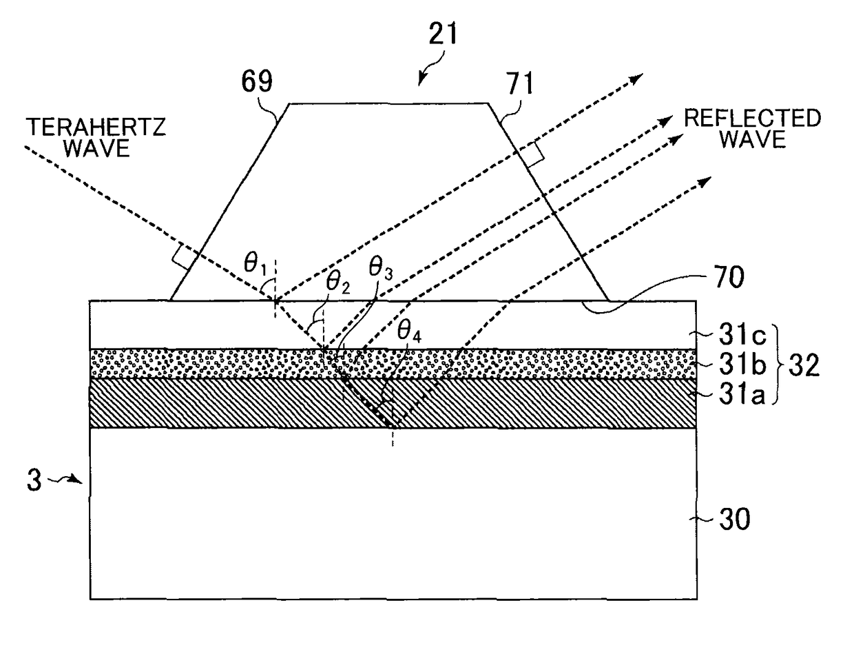
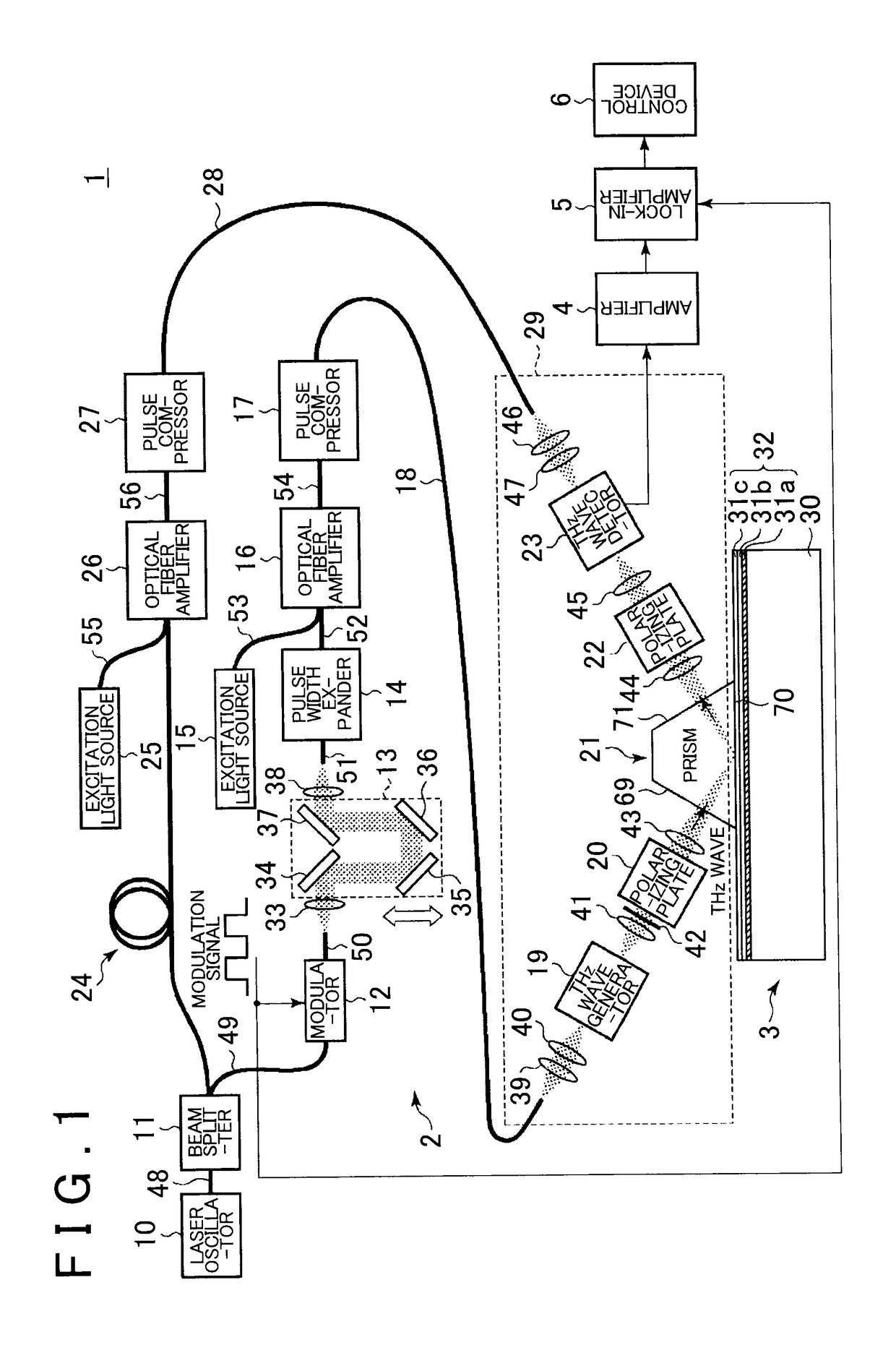
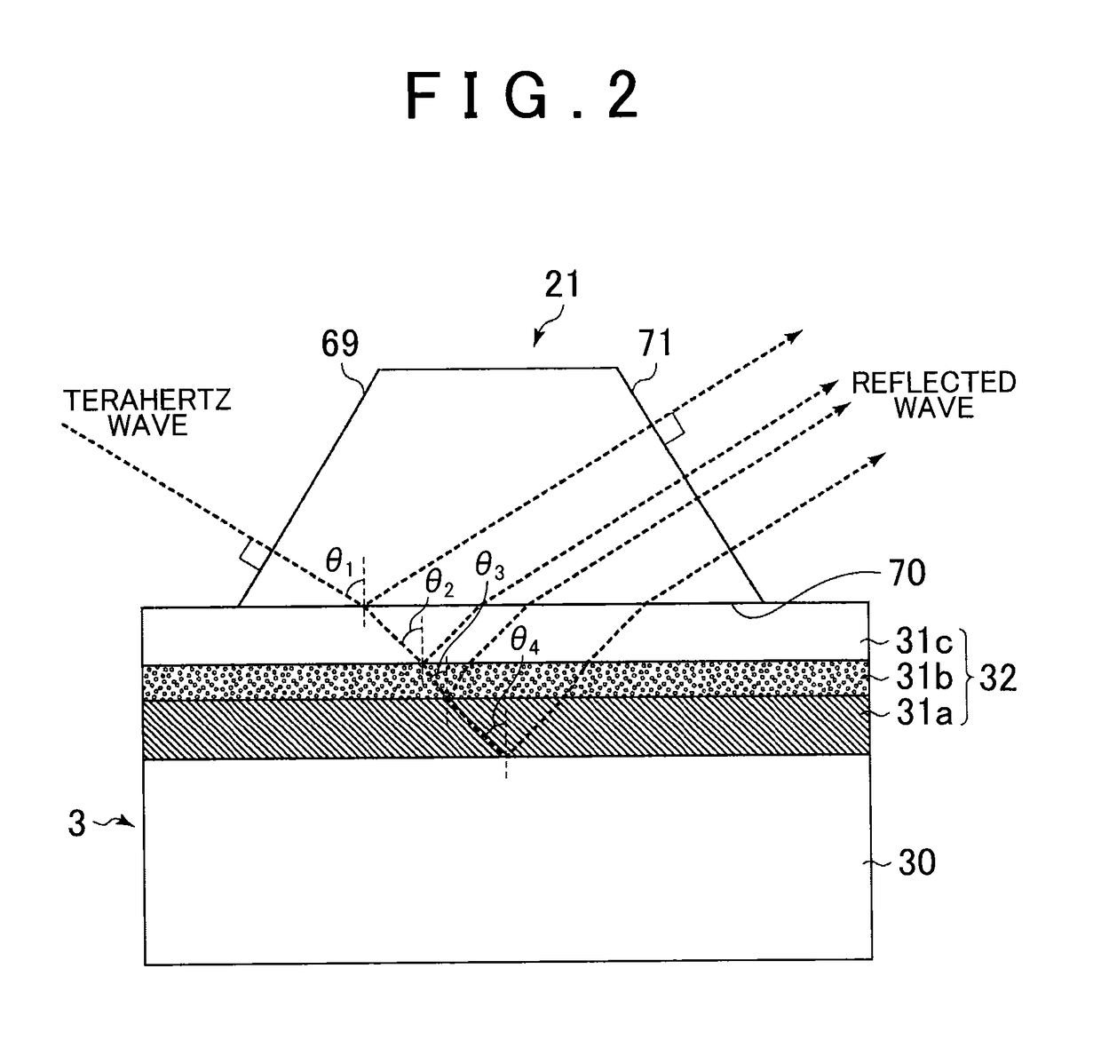
[0008]According to the invention, the terahertz wave is applied to the sample via the prism, and hence it is possible to cause the terahertz wave to enter the sample at a relatively large incident angle. Since it is possible to cause the terahertz wave to enter the sample at the relatively large incident angle, it is possible to make a significant difference between the time waveform of the S-polarization component in the reflected wave and the time waveform of the P-polarization component in the reflected wave. As a result, according to the embodiment, it is possible to measure the film thickness based on the difference between the time waveform of the S-polarization component in the reflected wave and the time waveform of the P-polarization component in the reflected wave more accurately and reliably.

Problems solved by technology

However, in the case where a film that causes dispersion or absorption of the terahertz wave is included in the multi-layer film, it is difficult to accurately measure the thickness of a film present below the film that causes the dispersion or absorption of the terahertz wave.

Method used


Image

  • Film thickness measuring device and film thickness measuring method
  • Film thickness measuring device and film thickness measuring method
  • Film thickness measuring device and film thickness measuring method

Examples


Embodiment Construction

[0028]FIGS. 18A and 18B are views each showing a reflected wave when a terahertz wave is applied to a sample. FIG. 18A is a view conceptually showing the reflected waves from individual layers, while FIG. 18B is a view showing a waveform in which the reflected waves from the individual layers are combined. A sample 30 is formed with a multi-layer film 32 having, e.g., a three-layer structure. A film 31a as the first layer is, e.g., a conductive primer layer. A film 31b as the second layer is, e.g., a metallic base layer. A film 31c as the third layer is, e.g., a clear layer. In the case where the terahertz wave is applied to the sample 3, reflected waves from four interfaces reach a terahertz wave detector 23. Since the sufficiently short terahertz wave is applied, the pulse width of a reflected wave 77a on the surface of the film 31c as the third layer becomes sufficiently short. In addition, the pulse width of a reflected wave 77b at an interface between the film 31c as the third ...


PUM


Abstract

A film thickness measuring device including: a terahertz wave generator; a prism that has an entrance surface, an abutment surface capable of abutting a surface of a sample including a first film on a side where the first film is formed, and an emission surface; a terahertz wave detector that detects an S-polarization component and a P-polarization component of a reflected wave from the sample, emitted from the emission surface of the prism; and a control section configured to determine a thickness of the first film formed in the sample, based on a difference between a time waveform of the S-polarization component of the reflected wave and a time waveform of the P-polarization component of the reflected wave.

Description

INCORPORATION BY REFERENCE[0001]The disclosure of Japanese Patent Application No. 2014-182859 filed on Sep. 9, 2014 including the specification, drawings and abstract is incorporated herein by reference in its entirety.BACKGROUND OF THE INVENTION1. Field of the Invention[0002]The invention relates to a film thickness measuring device and a film thickness measuring method.2. Description of Related Art[0003]Many industrial products are coated with multi-layer films. The individual multi-layer films have various functions such as rust prevention, adhesion attainment, chipping prevention, coloring, glossing, heat protection, and wear resistance attainment. In order to ensure these functions, it is necessary to accurately grasp the thickness of each layer. To cope with this, a technique for measuring the thickness of each layer of the multi-layer film nondestructively is proposed. Recently, a technique for measuring the thickness of each layer of the multi-layer film by using a terahertz...

Claims


Application Information

Patent Timeline
Patent Type & Authority Patents(United States)
IPC IPC(8): G01B11/06
CPCG01B11/0641
Inventor TAKAYANAGI, JUNOHTAKE, HIDEYUKIAIKYO, HIDEYUKIFUJISAWA, YASUNARINABESHIMA, ATSUO
Owner TOYOTA JIDOSHA KK
Learn More