Semiconductor Device Manufacturing Method and Plasma Oxidation Treatment Method

a technology of plasma oxidation treatment and semiconductor devices, which is applied in the direction of coatings, chemical vapor deposition coatings, electric discharge tubes, etc., can solve the problems of increased sheet resistance, increased leakage current, and product malfunction, so as to stabilize the quality of a semiconductor product, prevent the effect of affecting the product, and significantly reduce the contamination at atomic level

Inactive Publication Date: 2008-02-07
TOKYO ELECTRON LTD
View PDF4 Cites 30 Cited by
  • Summary
  • Abstract
  • Description
  • Claims
  • Application Information

AI Technical Summary

Benefits of technology

[0012]A second object is to suppress contamination of a semiconductor device due to a metal, such as tungsten, in the re-oxidation process, as far as possible.
[0013]A third object is to improve a re-oxidation process by use of a plasma processing apparatus of the RLSA type, so as to reliably perform the re-oxidation process without decreasing the oxide film thickness on the poly-silicon layer
[0037]Particularly, where a flow rate ratio of hydrogen gas relative to oxygen gas (which may be referred to as “H2 / O2 ratio” hereinafter) is set to be 8 or more, not only tungsten oxidation is prevented, but also tungsten contamination at atomic level is significantly reduced. Consequently, it is possible to stabilize the quality of a semiconductor product while preventing ill effects from being caused on the product.
[0038]Further, since tungsten contamination is reduced or suppressed, the interior of the chamber is maintained in a clean state. In this case, even where a re-oxidation process is repeatedly performed in the same chamber, it is possible to suppress a decrease in oxide film thickness, which is an inherent problem of re-oxidation processes performed by plasma processing apparatuses of the RLSA type.
[0039]Further, according to the present invention, it is possible to obtain the following advantages by use of a plasma processing apparatus of the RLSA type, as compared to a plasma processing apparatus of another type (for example, a plasma processing apparatus of the parallel-plate type or magnetron type.
[0040]Specifically, where a plasma processing apparatus of the RLSA type is used, plasma is generated with a high density and a low electron temperature, so an oxide film can be formed with higher quality and fewer damages, as compared to another plasma processing apparatus. Accordingly, an oxide film thus formed on a poly-silicon layer sidewall has quality much better than that of an oxide film formed by thermal oxidation processes. For example, even where the process is performed at a low temperature of about 400° C., the property concerning leakage current becomes better than that obtained by thermal oxidation processes.

Problems solved by technology

Conventionally, poly-silicon is used for gate electrodes, but entailing a disadvantage such that it increases the sheet resistance.
When a voltage is applied to the gate electrode, an electric field is concentrated at this exposed portion, which may cause malfunctions of the product, such as an increase in leakage current.
However, tungsten and tungsten silicide that are used for decreasing the sheet resistance of gate electrodes are rapidly oxidized when the temperature exceeds about 300° C. and about 400° C., respectively.
Thus, a problem arises such that the resistance of the gate electrode is increased.
Further, WO3 may be scattered and contaminate a wafer, thereby causing a problem in that the process yield for semiconductor devices is decreased.
In addition, thermal oxidation processes entail difficulty in forming an optimum sidewall oxide film of high quality, and need a relatively long time.
Consequently, thermal oxidation processes make it difficult not only to control formation of the oxide film but also to improve the throughput, thereby decreasing the productive efficiency.
However, this Document suggests no application to selective re-oxidation for a poly-silicon layer included in a gate electrode.
However, it has been found that, even if oxidation of the tungsten layer is suppressed, a large amount of tungsten is mixed into semiconductor devices as a metal contaminant at atomic level, and the contamination thus caused reaches a level not negligible for the performance of the semiconductor devices.
In other word, tungsten thus mixed may affect semiconductor devices, such as transistors, and cause malfunctions of the product, thereby decreasing the process yield.
However, it has been confirmed that, in the process of performing the re-oxidation process by use of the plasma processing apparatus of the RLSA type, if the chamber is contaminated with tungsten, oxidation of poly-silicon is inhibited and the thickness of an oxide film thus formed is decreased, although the mechanism for this is still unexplained.
However, if the oxide film thickness is decreased, semiconductor products suffer an increase in leakage current and so forth, which make it difficult to attain the original purpose of the re-oxidation.

Method used


Image

  • Semiconductor Device Manufacturing Method and Plasma Oxidation Treatment Method
  • Semiconductor Device Manufacturing Method and Plasma Oxidation Treatment Method
  • Semiconductor Device Manufacturing Method and Plasma Oxidation Treatment Method

Examples


Embodiment Construction

[0066]Preferable embodiments of the present invention will now be described with reference to the accompanying drawings.

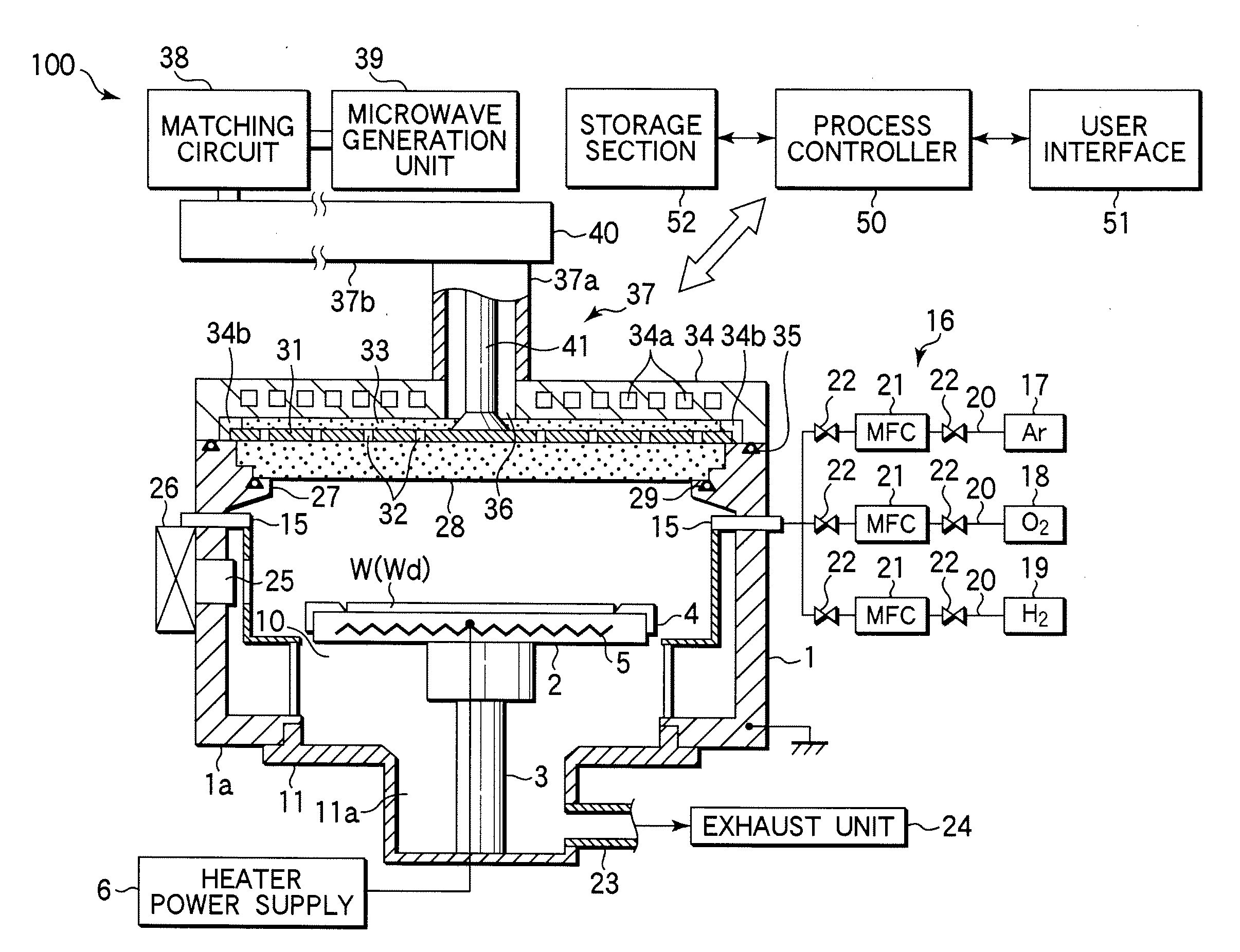
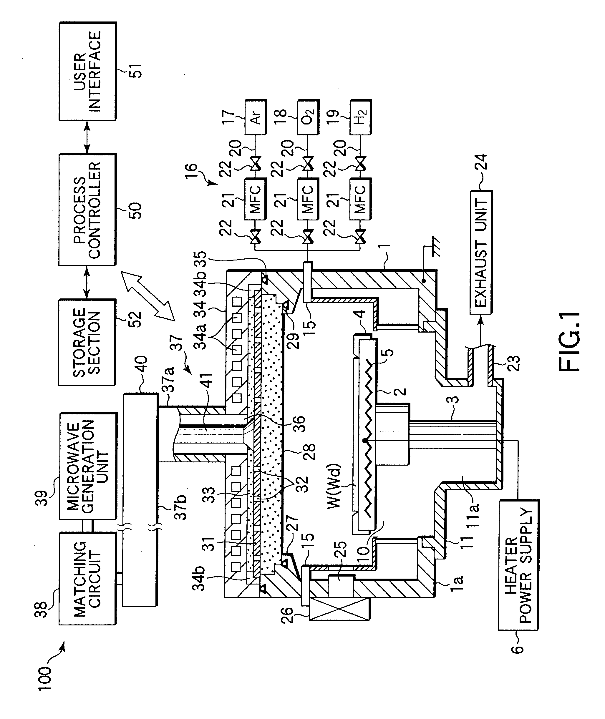
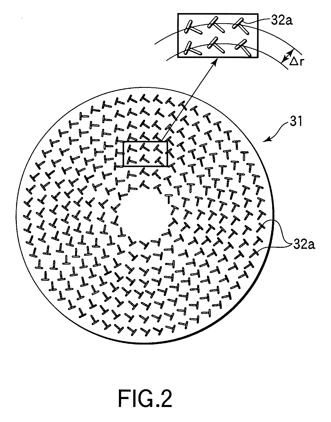
[0067]FIG. 1 is a sectional view schematically showing an example of a plasma processing apparatus suitable for performing a plasma oxidation method according to the present invention. This plasma processing apparatus utilizes an RLSA (Radial Line Slot Antenna) plasma generation technique, in which microwaves are supplied from a planar antenna having a plurality of slots into a process chamber to generate plasma, so that microwave plasma is generated with a high density and a low electron temperature.

[0068]This plasma processing apparatus 100 can proceed with a plasma process at a low temperature of 600° C. or less and free from damage to the underlying film and so forth. Further, this apparatus can provide high density plasma with good plasma uniformity to realize process uniformity comparable to those attained by diffusion furnaces. Accordingly, the plasma oxidat...


PUM

PropertyMeasurementUnit
temperatureaaaaaaaaaa
process temperatureaaaaaaaaaa
temperatureaaaaaaaaaa

Abstract

A selective oxidation process is performed on a gate electrode in a plasma processing apparatus 100. A wafer W with the gate electrode formed thereon is placed on a susceptor 2 within a chamber 1. Ar gas, H2 gas, and O2 gas are supplied from an Ar gas supply source 17, an H2 gas supply source 18, and an O2 gas supply source 19 in a gas supply system 16 through a gas feed member 15 into the chamber 1. At this time, a flow rate ratio H2 / O2 of H2 gas relative to O2 gas is set to be 1.5 or more and 20 or less, preferably to be 4 or more, and more preferably to be 8 or more. Further, the pressure inside the chamber is set to be 3 to 700 Pa, such as 6.7 Pa (50 mTorr).

Description

TECHNICAL FIELD [0001]The present invention relates to a method for manufacturing a semiconductor device by use of plasma in processing a semiconductor substrate, and further to a method for performing a plasma oxidation process.BACKGROUND ART [0002]In recent years, owing to the demands for higher integration degrees and higher operation speeds of LSIs, design rules for semiconductor devices that constitute LSIs are increasingly miniaturized. Along with this trend, the resistivity of transistor gate electrodes used in DRAMs, flash memories, and so forth is required to be lower. Conventionally, poly-silicon is used for gate electrodes, but entailing a disadvantage such that it increases the sheet resistance. Accordingly, it has been proposed to laminate a poly-silicon layer with a refractory metal, such as tungsten, or silicide of the metal, which is low in resistivity, high in adhesion to a silicon oxide film or silicon itself, and good in processability. Specifically, a tungsten po...

Claims


Application Information

Patent Timeline
Patent Type & Authority Applications(United States)
IPC IPC(8): H01L21/31C23C16/00
CPCH01J37/32192H01L21/28061H01L29/045H01L21/32105H01L21/28247
Inventor KABE, YOSHIROSASAKI, MASARU
Owner TOKYO ELECTRON LTD
Why Eureka
Try Eureka