Selective film deposition method to form air gaps

a film deposition and air gap technology, applied in the field of selective film deposition, can solve problems such as reducing the performance of devices

Active Publication Date: 2018-01-02
ASM IP HLDG BV
View PDF1633 Cites 294 Cited by
  • Summary
  • Abstract
  • Description
  • Claims
  • Application Information

AI Technical Summary

Problems solved by technology

The formation may involve an etching step, which may ca

Method used


Image

  • Selective film deposition method to form air gaps
  • Selective film deposition method to form air gaps
  • Selective film deposition method to form air gaps

Examples


Embodiment Construction

[0015]Although certain embodiments and examples are disclosed below, it will be understood by those in the art that the invention extends beyond the specifically disclosed embodiments and / or uses of the invention and obvious modifications and equivalents thereof. Thus, it is intended that the scope of the invention disclosed should not be limited by the particular disclosed embodiments described below.

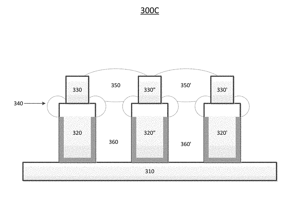
[0016]Selective deposition is desirable in order to grow particular features for a variety of applications. One particular feature, air gaps, has been used in 14 nm nodes, which currently is the smallest node size manufactured. Air gaps created in the 14 nm node may have, for example, a height of approximately 140 nm and a width of approximately 50 nm. This gap can be formed in a trench of approximately 180 nm in height, the trench herein meaning the space in between the metallization lines. The area of the air gap may be approximately 6,500 nm2, while the trench can have an area of 19...


PUM


Abstract

A method for depositing a film to form an air gap within a semiconductor device is disclosed. An exemplary method comprises pulsing a metal halide precursor onto the substrate and pulsing an oxygen precursor onto a selective deposition surface. The method can be used to form an air gap to, for example, reduce a parasitic resistance of the semiconductor device.

Description

FIELD OF INVENTION[0001]The present disclosure generally relates to processes for manufacturing electronic devices. More particularly, the disclosure relates to selectively forming films through atomic layer deposition (ALD) or chemical vapor deposition (CVD). Specifically, the disclosure discloses methods to form ALD or CVD films that can be used to form an air gap.BACKGROUND OF THE DISCLOSURE[0002]Generally, deposition of films has taken place in a manner such that layers are grown from the bottom in an upward direction. For example, a film grown on a wafer is often grown in a direction vertical to the wafer's surface. Other films may be grown vertically on a microstructure surface. Some examples of features created in this manner include trench filling, step formation, or FinFET features, for example.[0003]Air gaps are features with applicability in film deposition. U.S. Pat. No. 7,304,388 to Dubin et al. discloses air gaps that are created by first forming a sacrificial interlay...

Claims


Application Information

Patent Timeline
IPC IPC(8): H01L21/768H01L21/02
CPCH01L21/7682H01L21/02271H01L21/0228H01L21/02164H01L21/02167H01L21/02175H01L21/76832
Inventor ZHU, CHIYU
Owner ASM IP HLDG BV
Why Eureka
Try Eureka