Radiation-assisted selective deposition of metal-containing cap layers

a technology of metal-containing cap layers and selective deposition, which is applied in the direction of coatings, chemical vapor deposition coatings, metallic material coating processes, etc., can solve the problems of affecting the acceptance of this complex process, electromigration and stress migration have fast become critical challenges, and the defects that can destroy an integrated circui

Inactive Publication Date: 2010-08-19
TOKYO ELECTRON LTD
View PDF38 Cites 180 Cited by
  • Summary
  • Abstract
  • Description
  • Claims
  • Application Information

AI Technical Summary

Benefits of technology

[0006]Embodiments of the invention provide a method for forming metal-containing cap layers on patterned substrates, where the metal-containing cap layers are selectively on Cu metal surfaces relative to on dielectric layer surfaces. According to some embodiments, the metal-containing cap layer can contain ruthenium (Ru),

Problems solved by technology

The use of Cu metal in multilayer metallization schemes for manufacturing integrated circuits has created several problems that require solutions.
For example, high mobility of Cu atoms in dielectric materials and Si can result in migration of Cu atoms into those materials, thereby forming electrical defects that can destroy an integrated circuit.
Because electromigration and stress migration lifetimes are

Method used


Image

  • Radiation-assisted selective deposition of metal-containing cap layers
  • Radiation-assisted selective deposition of metal-containing cap layers
  • Radiation-assisted selective deposition of metal-containing cap layers

Examples


Embodiment Construction

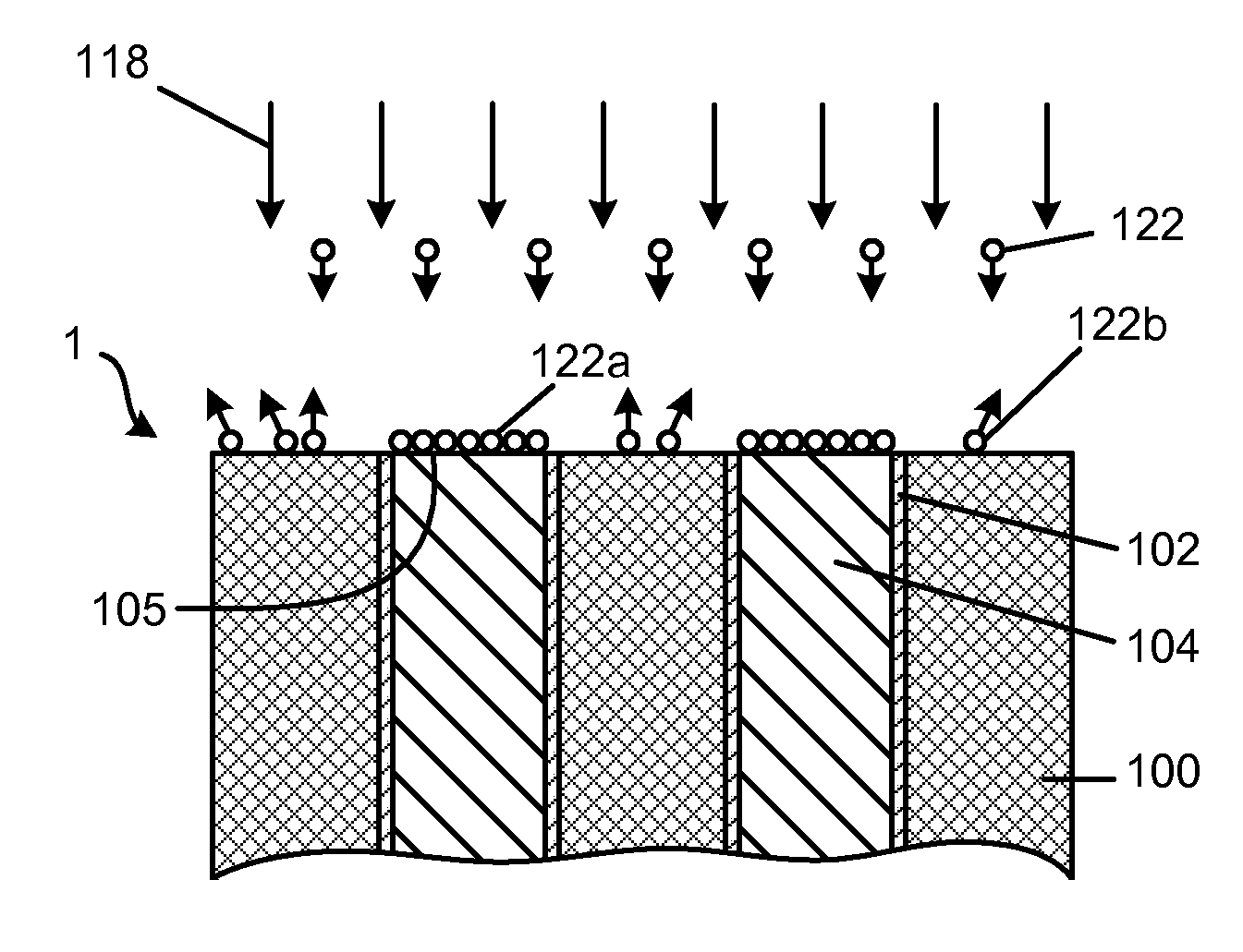
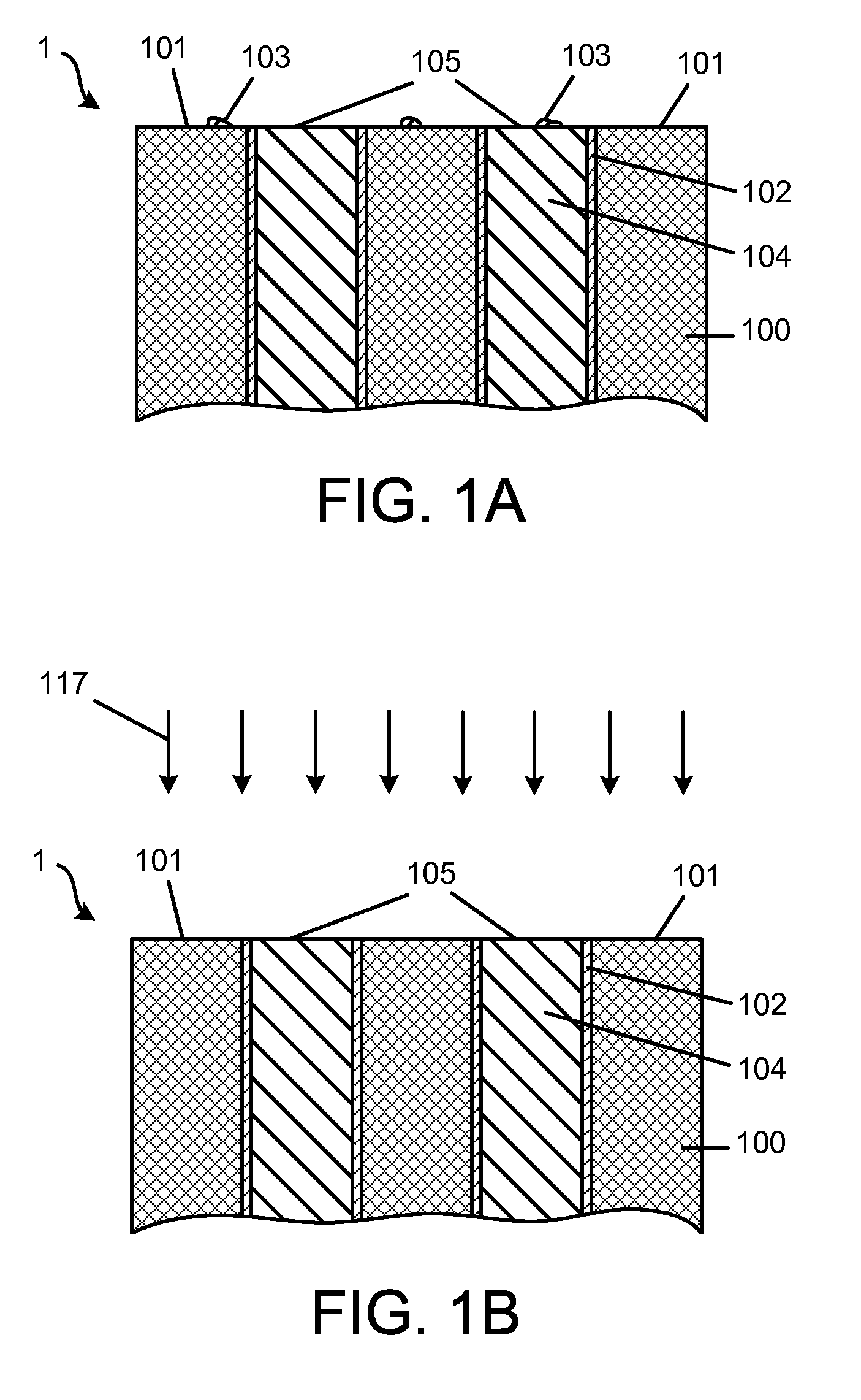
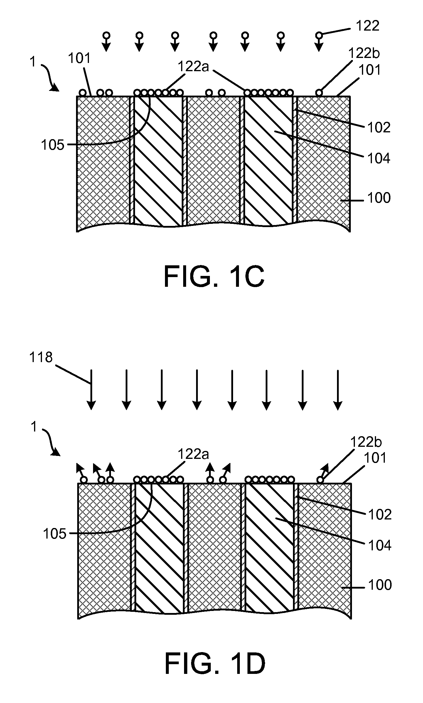
[0013]Embodiments of the invention provide methods for integrating metal-containing cap layers into Cu metallization of semiconductor devices to improve electromigration and stress migration in the devices. One skilled in the relevant art will recognize that the various embodiments may be practiced without one or more of the specific details, or with other replacement and / or additional methods, materials, or component. In other instances, well-known structures, materials, or operations are not shown or described in detail to avoid obscuring aspects of various embodiments of the invention. Similarly, for purposes of explanation, specific numbers, materials, and configurations are set forth in order to provide a thorough understanding of the invention. Furthermore, it is understood that the various embodiments shown in the figures are illustrative representations and are not necessary drawn to scale.

[0014]FIGS. 1A-1F show schematic cross-sectional views of formation of metal-containin...


PUM

PropertyMeasurementUnit
Nanoscale particle sizeaaaaaaaaaa

Abstract

A method for integrating metal-containing cap layers into copper (Cu) metallization of semiconductor devices to improve electromigration and stress migration in bulk Cu metal. In one embodiment, the method includes providing a patterned substrate containing Cu metal surfaces and dielectric layer surfaces, exposing the patterned substrate to a process gas comprising a metal-containing precursor, and irradiating the patterned substrate with electromagnetic radiation, where selective metal-containing cap layer formation on the Cu metal surfaces is facilitated by the electromagnetic radiation. In some embodiments, the method further includes pre-treating the patterned substrate with additional electromagnetic radiation and optionally a cleaning gas prior to forming the metal-containing cap layer.

Description

FIELD OF THE INVENTION[0001]The present invention relates to semiconductor processing and semiconductor devices, and more particularly, to a method of integrating metal-containing cap layers into copper(Cu) metallization of semiconductor devices to improve electromigration and stress migration in bulk Cu metal.BACKGROUND OF THE INVENTION[0002]An integrated circuit contains various semiconductor devices and a plurality of conducting metal paths that provide electrical power to the semiconductor devices and allow these semiconductor devices to share and exchange information. Within the integrated circuit, metal layers are stacked on top of one another using intermetal or interlayer dielectric layers that insulate the metal layers from each other. Normally, each metal layer must form an electrical contact to at least one additional metal layer. Such electrical contact is achieved by etching a hole (i.e., a via) in the interlayer dielectric that separates the metal layers, and filling t...

Claims


Application Information

Patent Timeline
IPC IPC(8): H01L21/3205
CPCC23C16/047C23C16/16C23C16/45523H01L21/02074H01L21/28562H01L21/76886H01L21/76846H01L21/76849H01L21/76862H01L21/76883H01L21/3205
Inventor ISHIZAKA, TADAHIROMIZUNO, SHIGERU
Owner TOKYO ELECTRON LTD
Why Eureka
Try Eureka