Underbump metallization structure

a technology of metallization structure and bump pad, which is applied in the direction of semiconductor devices, semiconductor/solid-state device details, electrical devices, etc., can solve the problems of yield and overall productivity problems, shear stress and shear stress building up along the interface, etc., to prevent or reduce delamination and device failure

Active Publication Date: 2018-01-02
TAIWAN SEMICON MFG CO LTD
View PDF13 Cites 2 Cited by
  • Summary
  • Abstract
  • Description
  • Claims
  • Application Information

AI Technical Summary

Benefits of technology

[0010]An advantage of a preferred embodiment of the present invention is that stresses caused by differences in materials' coefficient of thermal expansion are absorbed by the passivation layer and are not transmitted further into the structure, thereby helping to prevent or reduce delamination and device failure.

Problems solved by technology

As such, when the temperature of these materials is raised, for example during a flip chip bond reflow process, the different materials will expand to different lengths, causing peeling stress and shear stress to build up along the interfaces.
These stresses could easily lead to delamination, such as delamination between the UBM and the contact pad, which would immediately cause problems in yield and overall productivity.
This problem is especially true when low-k and extremely low-k dielectrics are utilized for one or more of the dielectric layers.

Method used


Image

  • Underbump metallization structure
  • Underbump metallization structure
  • Underbump metallization structure

Examples


Embodiment Construction

[0020]The making and using of the presently preferred embodiments are discussed in detail below. It should be appreciated, however, that the present invention provides many applicable inventive concepts that can be embodied in a wide variety of specific contexts. The specific embodiments discussed are merely illustrative of specific ways to make and use the invention, and do not limit the scope of the invention.

[0021]The present invention will be described with respect to preferred embodiments in a specific context, namely an under bump metallization (UBM) in connection with a contact pad. The invention may also be applied, however, to other types of electrical connections.

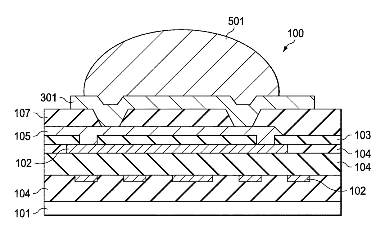
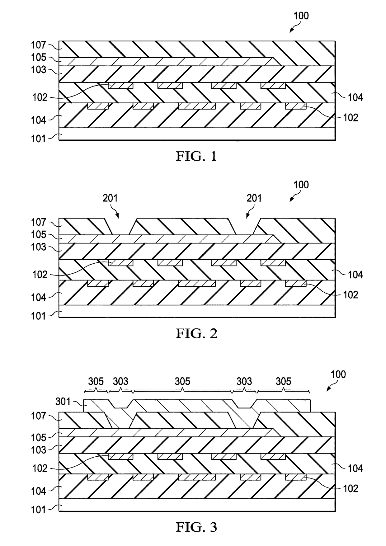
[0022]With reference now to FIG. 1, there is shown a portion of a semiconductor device 100 including a substrate 101 with a first passivation layer 103, a contact pad 105, and a second passivation layer 107 over the substrate 101. The substrate 101 preferably comprises a semiconductor base material upon which acti...


PUM


Abstract

A system and method for forming an underbump metallization (UBM) is presented. A preferred embodiment includes a raised UBM which extends through a passivation layer so as to make contact with a contact pad while retaining enough of the passivation layer between the contact pad and the UBM to adequately handle the peeling and shear stress that results from CTE mismatch and subsequent thermal processing. The UBM contact is preferably formed in either an octagonal ring shape or an array of contacts.

Description

[0001]This application claims the benefit of U.S. Provisional Patent Application Ser. No. 61 / 147,397, filed on Jan. 26, 2009, and entitled “Underbump Metallization Structure,” which application is incorporated herein by reference.TECHNICAL FIELD[0002]The present invention relates generally to a system and method of manufacturing semiconductor devices, and more particularly to a system and method for bump pad structures.BACKGROUND[0003]Generally, a bump may be formed on a semiconductor die in order to connect the semiconductor die to other dies or devices. These bumps are normally connected to the semiconductor die by layers of conductive material collectively known as under bump metallization (UBM) that extend through a first passivation layer. The UBM provides for a connection between the bump and a contact pad in order to electrically connect the bump to the various metal layers formed within the semiconductor die. The various metal layers are preferably separated by dielectric la...

Claims


Application Information

Patent Timeline
Patent Type & Authority Patents(United States)
IPC IPC(8): H01L23/488H01L23/00H01L23/31
CPCH01L24/05H01L23/3157H01L24/03H01L24/11H01L24/13H01L2224/0215H01L2224/02125H01L2224/0345H01L2224/03462H01L2224/0401H01L2224/0508H01L2224/05018H01L2224/05027H01L2224/05096H01L2224/05147H01L2224/05155H01L2224/05166H01L2224/05171H01L2224/05541H01L2224/05552H01L2224/05553H01L2224/05557H01L2224/05558H01L2224/05566H01L2224/05569H01L2224/05572H01L2224/05573H01L2224/05644H01L2224/05647H01L2224/05655H01L2224/1132H01L2224/1145H01L2224/11334H01L2224/11462H01L2224/11849H01L2224/13005H01L2224/13007H01L2224/13111H01L2224/13139H01L2224/13147H01L2924/00013H01L2924/01006H01L2924/01013H01L2924/01019H01L2924/01022H01L2924/01029H01L2924/01033H01L2924/01047H01L2924/01074H01L2924/01078H01L2924/01079H01L2924/01082H01L2924/05042H01L2924/05442H01L2924/00014H01L2924/2064H01L2224/13099H01L2224/05099H01L2224/13599H01L2224/05599H01L2224/29099H01L2224/29599
Inventor LIU, YU-WENTSAI, HAO-YICHEN, HSIEN-WEIJENG, SHIN-PUUCHEN, YING-JUHOU, SHANG-YUNTSAO, PEI-HAWYU, CHEN-HUA
Owner TAIWAN SEMICON MFG CO LTD
Why Eureka
Try Eureka