Integrated circuit package with transparent encapsulant and method for making thereof

a technology of integrated circuits and transparent encapsulants, which is applied in the direction of electrical equipment, semiconductor devices, semiconductor/solid-state device details, etc., can solve the problems of difficult to apply ceramic sealant b>1/b>, and difficult to achieve desired sealant effect, etc., to achieve easy application of transparent encapsulants, prevent or reduce delamination of transparent encapsulants, and reliable and durable

Inactive Publication Date: 2005-08-04
CARSEM M
View PDF44 Cites 75 Cited by
  • Summary
  • Abstract
  • Description
  • Claims
  • Application Information

AI Technical Summary

Benefits of technology

[0015] Many benefits are achieved by way of the present invention over conventional techniques. Certain embodiments of the present invention provide IC packages with transparent encapsulants. For example, the transparent encapsulants are both reliable and durable. Some embodiments of the present invention provide a method that can easily apply transparent encapsulants. Certain embodiments of the present invention can prevent or reduce delamination of transparent encapsulants. For example, the delamination of transparent encapsulants may occur during cooling and result in warpage and delamination rejects of the IC packages. Some embodiments of the present invention use stress-relief structures in a leadframe. The stress-relief structures can prevent or reduce the propagation of delamination of transparent encapsulants. Certain embodiments of the present invention apply transparent encapsulants to only one side of a leadframe. The amount of transparent encapsulant used is reduced and the fabrication costs are lowered. Some embodiments of the present invention provide transparent IC packages with improved heat dissipation, smaller size, and / or lighter weight. Certain embodiments of the present invention use matrix arrays of packaging units. These packaging units are singulated as an individual optical devices and / or packages. For example, the matrix arrays allow the use of a single mould for making packages of various sizes and shapes. Some embodiments of the present invention provide locking mechanisms. For example, the locking mechanisms include extended parts. During encapsulation, the heat causes the encapsulants to melt and flow under the extended parts. After cooling, the encapsulants under the locking mechanisms can prevent or reduce the delamination of transparent encapsulants

Problems solved by technology

For example, the fabrication process for coating the ceramic sealant 16 on the lower side of the ceramic upper plate 15 is complex and costly.
Additionally, the desired sealant effect is difficult to achieve between the ceramic upper plate 15 and the window sealant 17.
If the window 10 is peeled off from the ceramic upper plate 15, the IC package 1 can be significantly damaged.
Such disassociation often leads to cracks and thereby damages the IC package.

Method used


Image

  • Integrated circuit package with transparent encapsulant and method for making thereof
  • Integrated circuit package with transparent encapsulant and method for making thereof
  • Integrated circuit package with transparent encapsulant and method for making thereof

Examples


Embodiment Construction

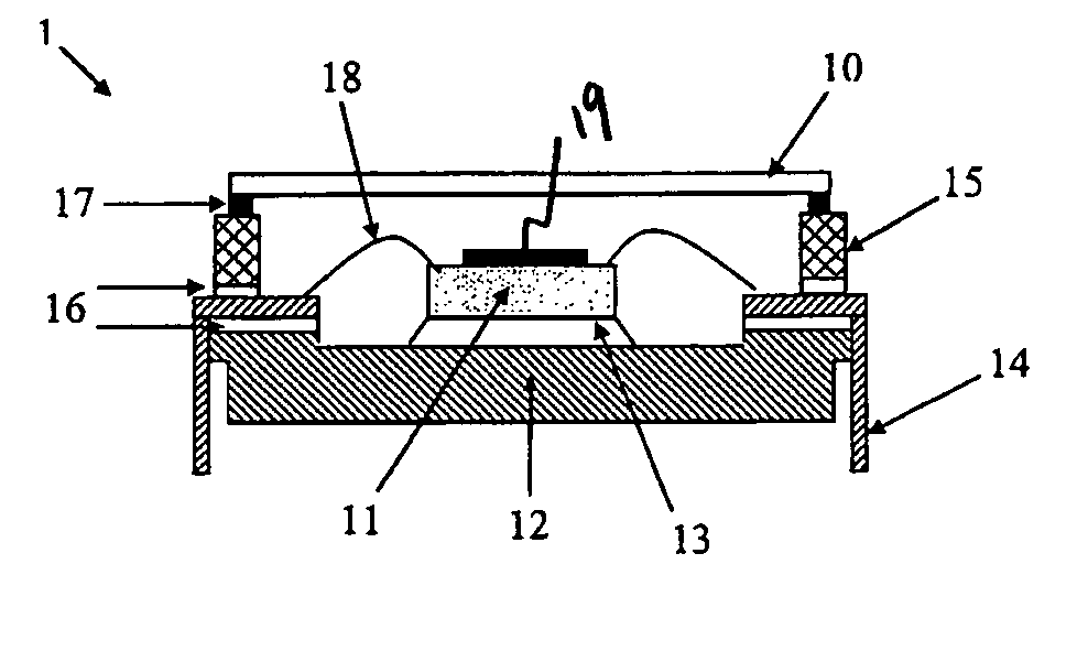
[0024] The present invention relates in general to integrated circuit (IC) packaging. More particularly, the invention provides an IC package with transparent encapsulant and a method for making thereof. Merely by way of example, the invention is described as it applies to a package in compliance with certain JEDEC standard, but it should be recognized that the invention has a broader range of applicability.

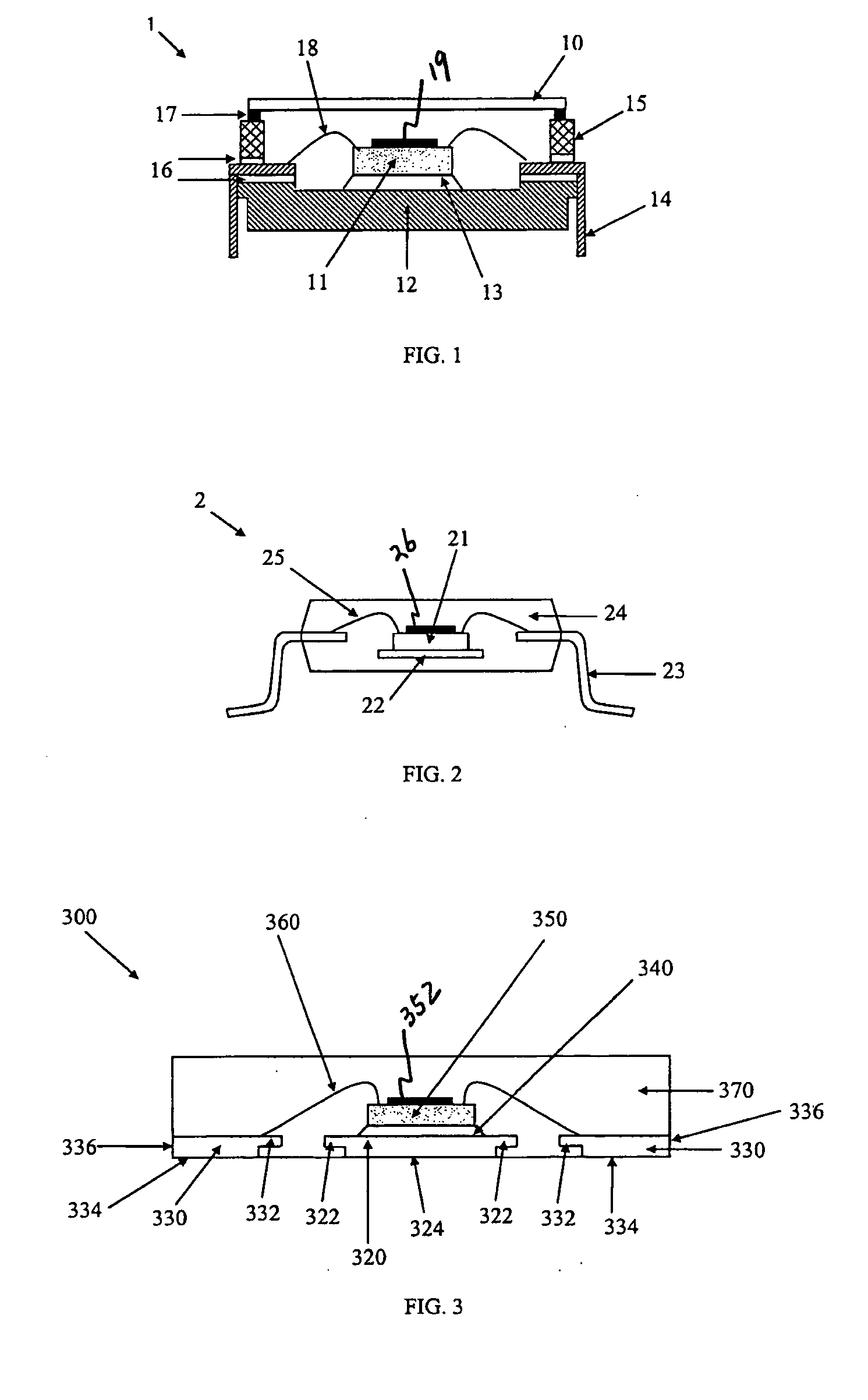
[0025]FIG. 3 is a simplified cross section of an IC package according to an embodiment of the present invention. This diagram is merely an example, which should not unduly limit the scope of the claims. One of ordinary skill in the art would recognize many variations, alternatives, and modifications. An IC package 300 includes a die pad 320, leads 330, a bonding layer 340, a die 350, conductive wires 360, and encapsulant material 370. Although the above has been shown using a selected group of components for the IC package 300, there can be many alternatives, modifications, and ...


PUM


Abstract

IC package with transparent encapsulant and method for making thereof. The IC package includes a die pad including a pad bottom surface, a die disposed on the die pad and including an integrated circuit, a plurality of leads including a plurality of lead bottom surfaces, a plurality of conductive wires connecting the die and the plurality of leads, and an encapsulant material. The encapsulant material is transparent for visible wavelengths. The pad bottom surface is exposed without being covered by the encapsulant material, and the plurality of lead bottom surfaces each are exposed without being covered by the encapsulant material.

Description

CROSS-REFERENCES TO RELATED APPLICATIONS [0001] This application claims priority to Malaysian Patent Application No. PI 20035051, filed Dec. 31, 2003, commonly assigned and incorporated by reference herein for all purposes. STATEMENT AS TO RIGHTS TO INVENTIONS MADE UNDER FEDERALLY SPONSORED RESEARCH OR DEVELOPMENT [0002] NOT APPLICABLE REFERENCE TO A “SEQUENCE LISTING,” A TABLE, OR A COMPUTER PROGRAM LISTING APPENDIX SUBMITTED ON A COMPACT DISK. [0003] NOT APPLICABLE BACKGROUND OF THE INVENTION [0004] The present invention relates in general to integrated circuit (IC) packaging. More particularly, the invention provides an IC package with transparent encapsulant and a method for making thereof. Merely by way of example, the invention is described as it applies to a package in compliance with certain JEDEC standard, but it should be recognized that the invention has a broader range of applicability. [0005] Integrated circuits are usually packaged before being used in electronic syste...

Claims


Application Information

Patent Timeline
Patent Type & Authority Applications(United States)
IPC IPC(8): H01L23/31H01L23/495
CPCH01L23/3107H01L24/48H01L24/97H01L27/14618H01L2224/32225H01L2224/32245H01L2224/48091H01L2224/48247H01L2224/73265H01L2224/97H01L2924/01012H01L2924/01029H01L2924/01078H01L2924/01079H01L2924/01082H01L2924/16195H01L23/49548H01L2924/01005H01L2924/01006H01L2924/01019H01L2924/01033H01L2924/00014H01L2224/85H01L2224/83H01L2924/00H01L2924/00012H01L2924/181H01L2924/12042H01L24/73H01L2924/14H01L2924/18301H01L2224/45099H01L2224/45015H01L2924/207
Inventor KHOR, LEK AHLEE, HUAT KOCKCHAN, MENG BOONTHUM, KONG MINTUNG, MUN HONGCHEONG, TUCK MUN
Owner CARSEM M
Why Eureka
Try Eureka