

Internal envelope infrastructure for electrical devices
a technology for electrical devices and envelope infrastructure, applied in lighting safety devices, semiconductor devices of light sources, lighting and heating apparatus, etc., can solve the problems of conductive pattern naturally breaking and electric devices cannot be operated, and achieve the effect of improving the current state of art and minimizing the risk of human exposur
- Summary
- Abstract
- Description
- Claims
- Application Information
AI Technical Summary
Benefits of technology
Problems solved by technology
Method used
Image

Examples
Embodiment Construction
[0028]The present invention will now be described more fully hereinafter with reference to the accompanying drawings, in which currently preferred embodiments of the invention are shown. This invention may, however, be embodied in many different forms and should not be construed as limited to the embodiments set forth herein; rather, these embodiments are provided for thoroughness and completeness, and fully convey the scope of the invention to the skilled person.
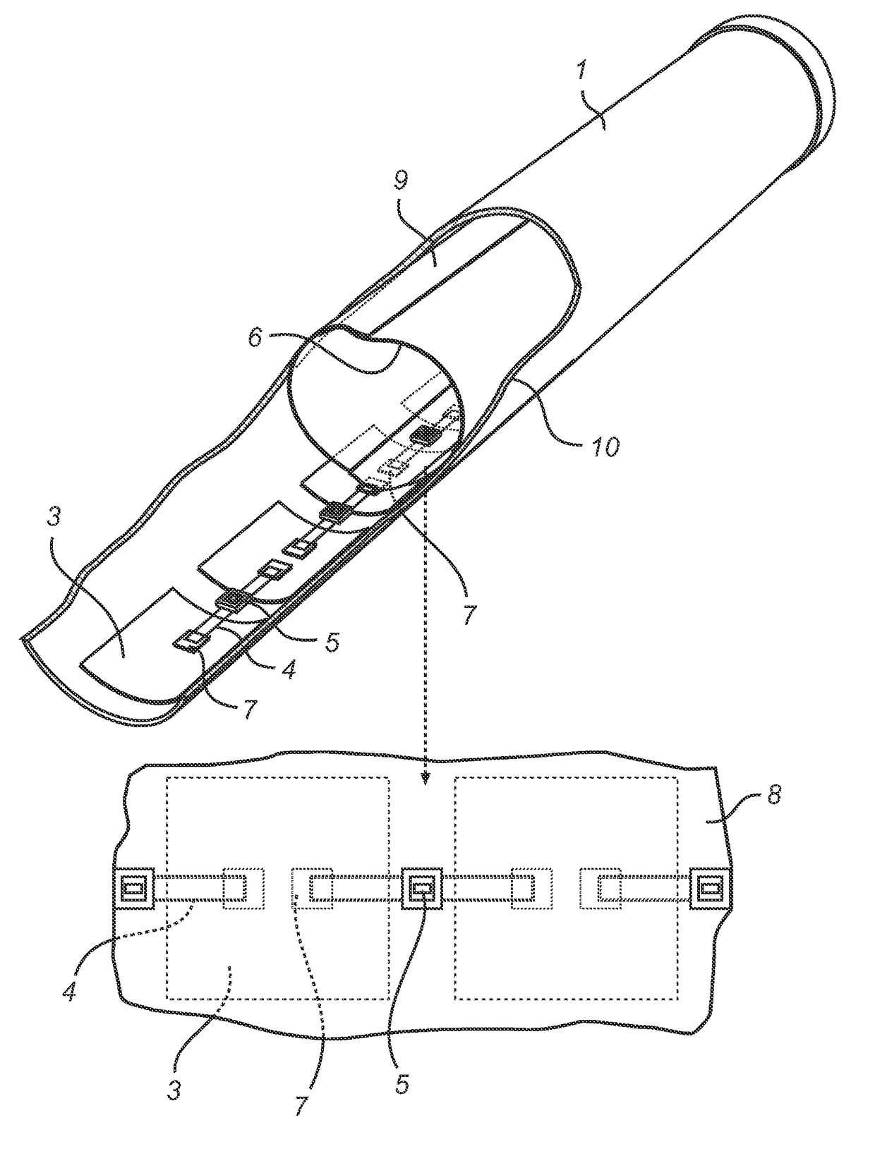
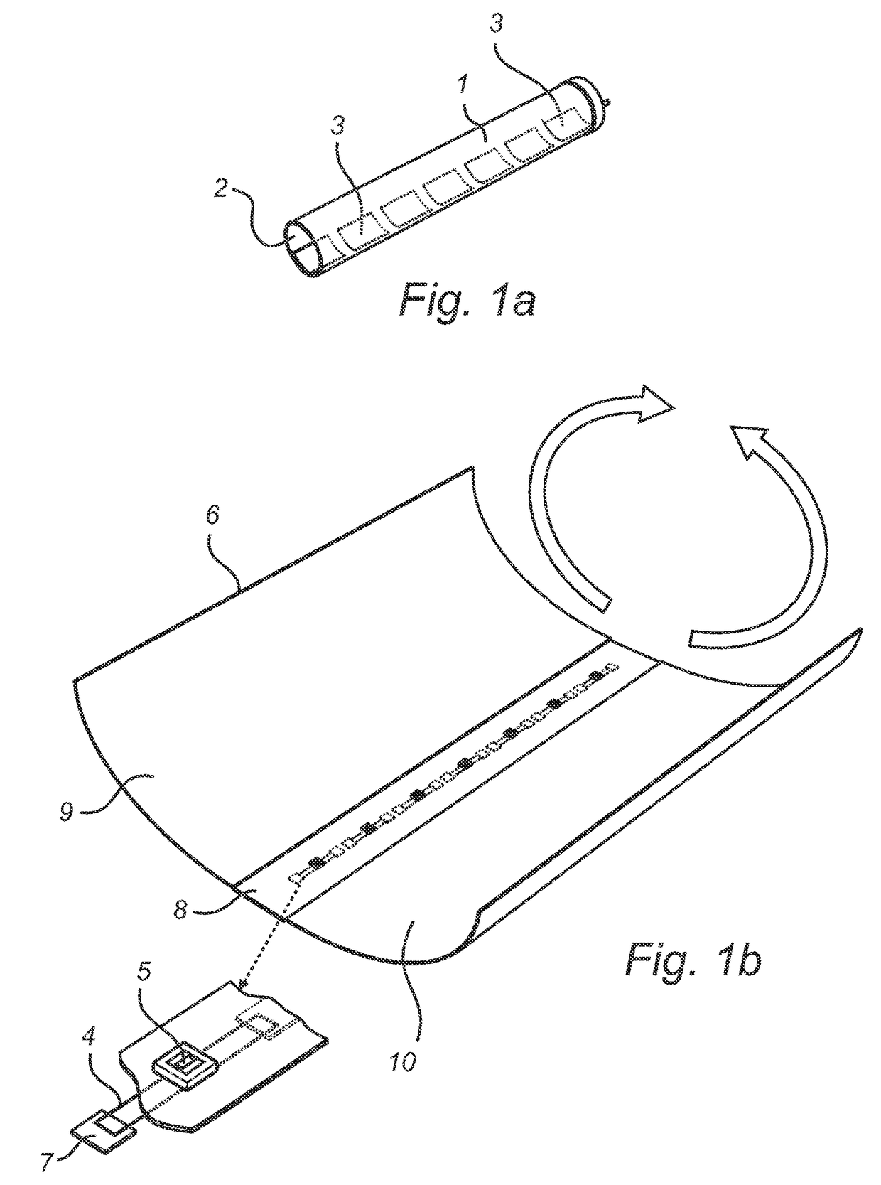
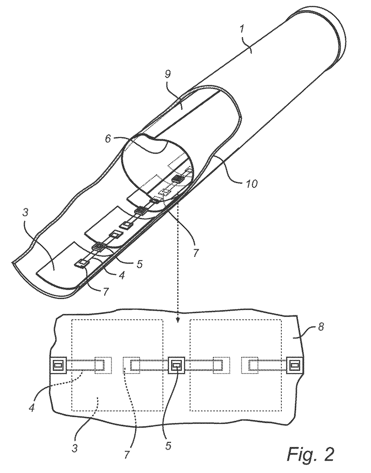
[0029]FIG. 1a shows one embodiment of a housing 1 according to the present invention. The housing has a coated conductive pattern 3 on the inside of the housing wall 2. The coated conductive pattern 3 is designed to provide the missing pieces or electrical bridging to an electrical device that is inserted into the housing. The conductive pattern 3 alone thus does not provide a continuous electrical interconnection but comprises a pattern of electrically separated or isolated electrical tracks or bridges. The housing 1 in FI...
PUM
| Property | Measurement | Unit |
|---|---|---|
| thickness | aaaaa | aaaaa |
| conductive | aaaaa | aaaaa |
| spring force | aaaaa | aaaaa |
Abstract
Description
Claims
Application Information