

Forming polysilicon structures
A technology of polysilicon and semiconductors, applied in semiconductor devices, semiconductor/solid-state device manufacturing, electrical components, etc., can solve problems such as etching deviation
- Summary
- Abstract
- Description
- Claims
- Application Information
AI Technical Summary
Problems solved by technology
Method used
Image

Examples
Embodiment Construction
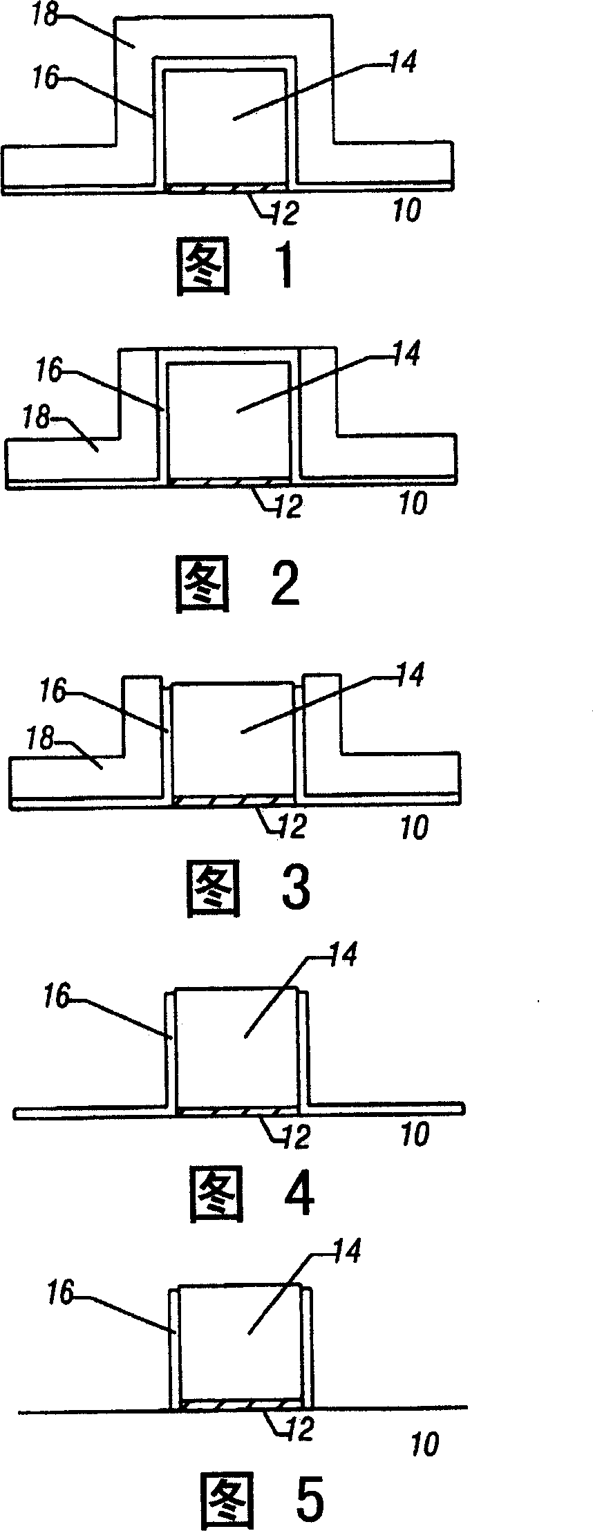
[0013] Referring to FIG. 1, a semiconductor substrate may have a polysilicon material formed on a suitable gate dielectric. The substrate may be, for example, a silicon substrate, and the gate dielectric may be, for example, oxide. Then, as shown in FIG. 1 , the polysilicon material may be patterned to form polysilicon gate material on gate dielectric 12 , all of which are disposed above substrate 10 . Because the polysilicon material is undoped or substantially undoped when etched, it can be easily etched and patterned to define the shape shown in FIG. 1 .
[0014] "Substantially undoped" is used to describe a polysilicon material that is either undoped, or doped at a level substantially lower than that of doped polysilicon that is utilized to form N-type or P-type The doping level of the gate electrode. Typically, these gate electrodes are considered heavily doped and have a doping concentration higher than 1E18 atoms per cubic centimeter.
[0015] Gate material 14 may be...
PUM
 Abstract
Description
Claims
Application Information