Method and device for deciding semiconductor making process state and semiconductor making device
A technology for manufacturing a device and a semiconductor, which is applied in the field of devices with means for measuring etching depth, and can solve the problems of difficulty in adjusting the etching state, difficulty in processing semiconductors with high precision, and insufficient consideration for reduction.
- Summary
- Abstract
- Description
- Claims
- Application Information
AI Technical Summary
Problems solved by technology
Method used
Image

Examples
Embodiment Construction
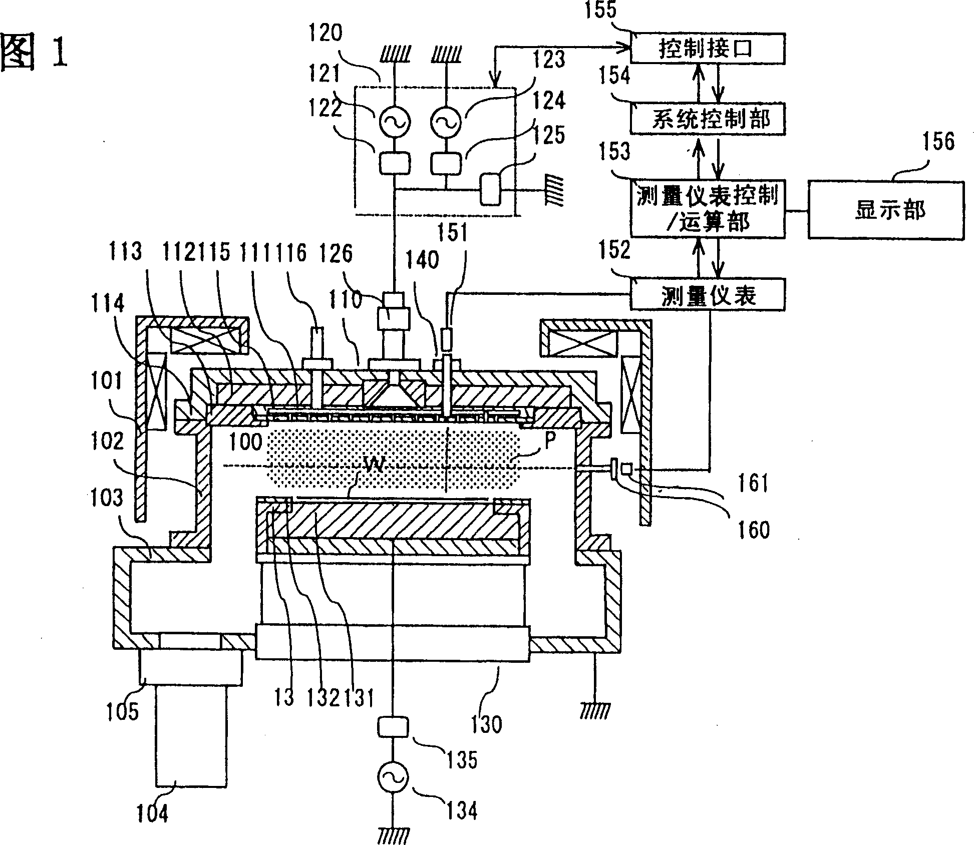
[0028] Hereinafter, embodiments of the present invention will be described with reference to the drawings.
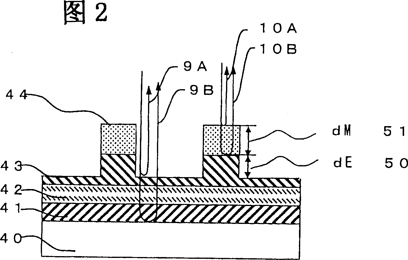
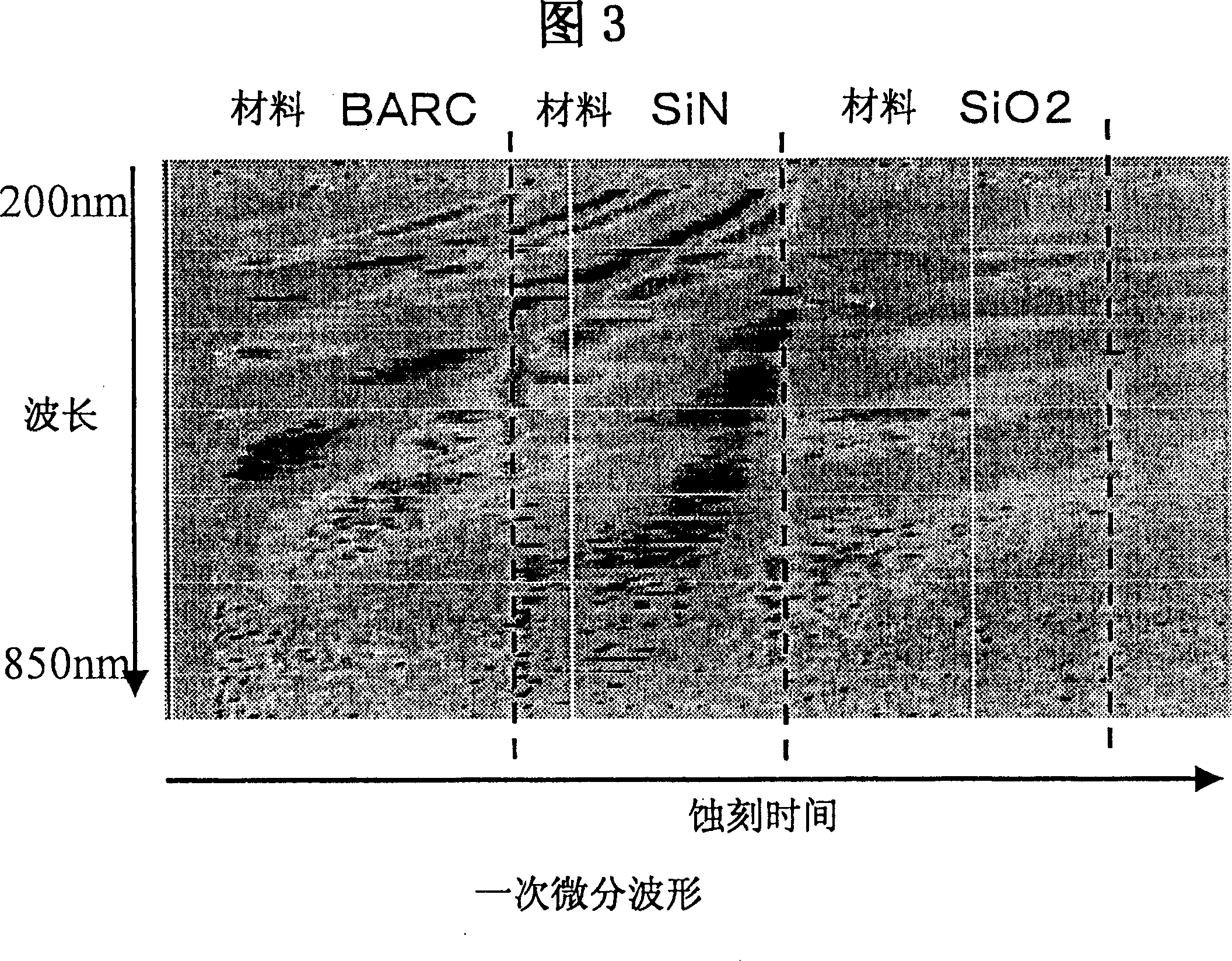
[0029] In addition, in each of the following embodiments, components having the same functions as in the first embodiment are given the same symbols as in the first embodiment, and detailed description thereof will be omitted. In the following examples, a method for measuring the amount of etching (etching depth and film thickness) in the etching process of the material to be processed will be described with respect to the method for judging the end point of the semiconductor device manufacturing process of the present invention. However, the present invention is not limited thereto, and can also be applied to methods of measuring film formation (film formation thickness) and the like in thin film processes formed by plasma CVD, sputtering, and the like.
[0030] Hereinafter, a first embodiment of the present invention will be described with reference to FIGS. 1 to 4 . ...
PUM
 Abstract
Description
Claims
Application Information