Shielding plate for enhancing flow field uniformity

A shielding plate and uniformity technology, which is applied in the field of microelectronics, can solve problems such as uneven etching rate, and achieve the effects of improving distribution uniformity, improving flow field uniformity, and reducing pressure difference

Active Publication Date: 2008-03-26
BEIJING NAURA MICROELECTRONICS EQUIP CO LTD
View PDF4 Cites 0 Cited by
  • Summary
  • Abstract
  • Description
  • Claims
  • Application Information

AI Technical Summary

Problems solved by technology

Although these structures have a certain effect on improving the uniformity of etching, most of the current etching equipment still faces the problem of uneven etching rate.

Method used


Image

  • Shielding plate for enhancing flow field uniformity
  • Shielding plate for enhancing flow field uniformity
  • Shielding plate for enhancing flow field uniformity

Examples


Embodiment Construction

[0028] The specific implementation of the shielding plate for improving flow field uniformity of the present invention will be described in further detail below in conjunction with the accompanying drawings, but it is not used to limit the scope of protection of the present invention.

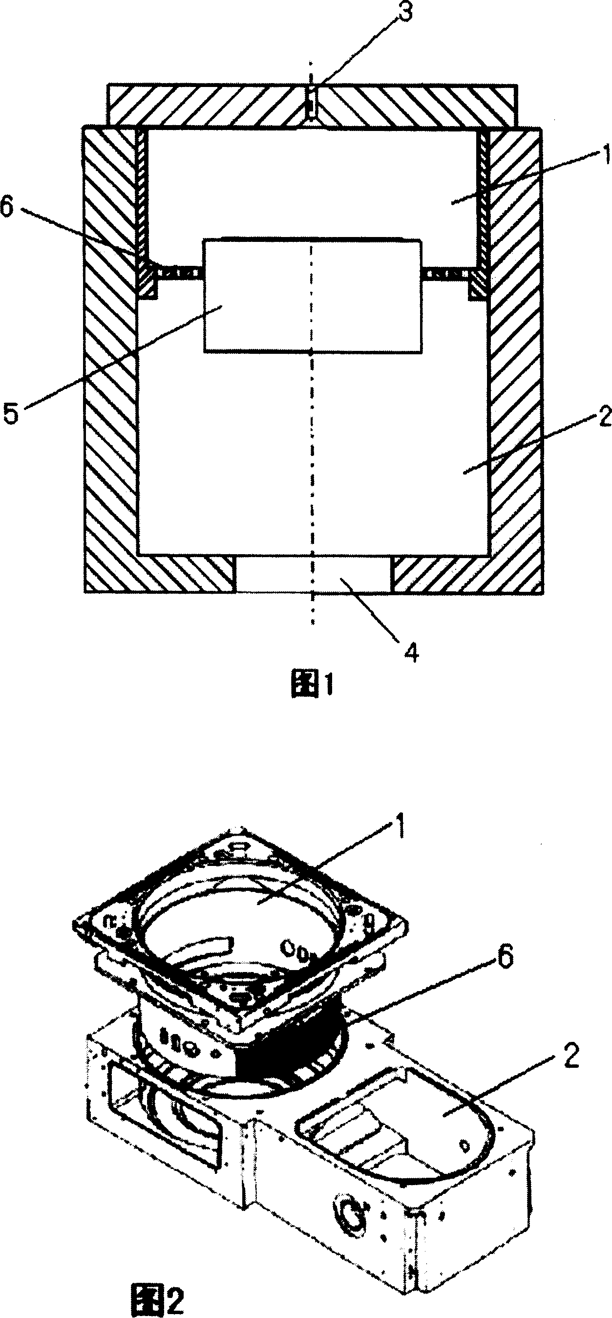
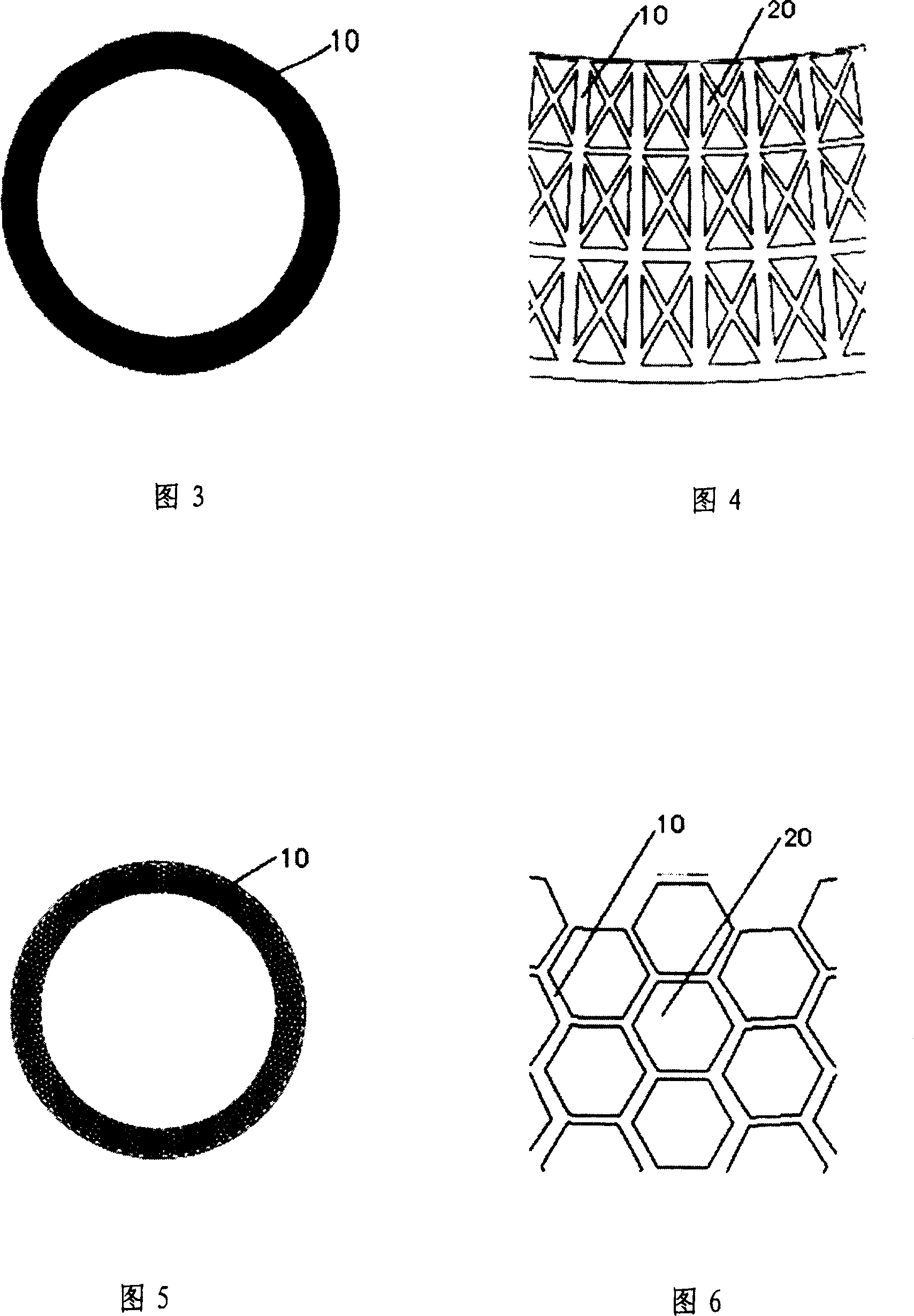
[0029] See Figures 3 and 4. The structure of the first embodiment of the shielding plate for improving the uniformity of the flow field of the present invention includes an annular plate body 1, on which a number of air holes are radially distributed from the center to the circumferential direction, and some air holes are formed from the plate body. 1 The center gradually becomes larger toward the circumference. The cross-sectional shape of the air hole is quadrilateral, and in each quadrilateral hole, a partition is respectively arranged along the two diagonals of the quadrilateral, and the quadrilateral air hole is divided into four triangular air holes, and the longitudinal section of each t...


PUM


Abstract

The invention relates to the shielding board used in the craftwork of chiseling and eroding the semiconductor. The invention is the shielding board building the equality of the flowing field, it includes the board body. The said board body is the form formed ringwise. The some air hole are distributed on the said board body presenting the emitting form from the center to the direction of the circle, the some air hole is bigger gradually the direction from the center of the board body to the circle. The availability of the invention is: because of the some air holes distributing from the center to the circle on the board body and becoming bigger gradually along the direction from the center to the circle, the flowing route in the inner of the reactive cavity of the air can be altered, the disturbing equality of the air in the inner of the reactive cavity can be improved, the corroding rate of the points of the surface of the silicon is make to be more close. The technical project of the invention can control the corroding rate and the equality in the range from the center of the wafer to the edge of the wafer can well even with the accretion of the size of the wafer.

Description

technical field [0001] The invention relates to the technical field of microelectronics, in particular to a shielding plate used in a semiconductor etching process. Background technique [0002] Semiconductor manufacturing technology includes the deposition of metals, dielectrics and other semiconductor materials, the etching of the above materials, and the removal of photoresist mask layers. In the etching process, plasma etching technology is widely used in etching processes such as gate etching, dielectric etching, and metal etching. A typical plasma etching reaction chamber includes a chamber, a plasma generation and control device, a process gas delivery device, a wafer chuck for wafer fixing, and Process Kits, which are used to control and limit gas flow and plasma The area where the body exists, and avoid the adsorption and deposition of etching products on the inner wall of the chamber that is not easy to disassemble and clean), etc. [0003] Under low pressure, th...

Claims


Application Information

Patent Timeline
Patent Type & Authority Patents(China)
IPC IPC(8): C23F4/04H01L21/3065
Inventor 林盛
Owner BEIJING NAURA MICROELECTRONICS EQUIP CO LTD
Why Eureka
Try Eureka