Assembly of FPC and PCB
A component and gold finger technology, applied in electrical components, printed circuit components, structural connections of printed circuits, etc., can solve problems such as low welding efficiency, affecting product welding quality, and difficult to effectively bridge FPC and PCB.
- Summary
- Abstract
- Description
- Claims
- Application Information
AI Technical Summary
Problems solved by technology
Method used
Image
Examples
Embodiment Construction
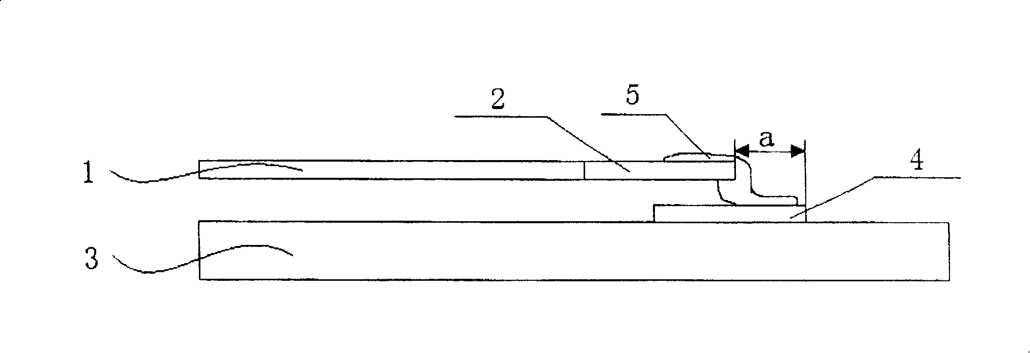
[0009] A FPC and PCB assembly, such as figure 1 As shown, it includes an FPC substrate 1, a gold finger 2 disposed on the end side of the FPC substrate, a PCB 3 and a gold finger 4 located on the end side of the PCB, the gold finger 2 on the FPC substrate extends from the outside to the inside of the FPC substrate 1, and on the FPC substrate The front end of gold finger 2 is set back relative to the front end of gold finger 4 on the PCB and is connected by soldering.
[0010] The golden fingers on the FPC substrate are formed by scraping off the insulating glue on the end side of the FPC substrate.
[0011] In the existing structure where the front end of the gold finger on the FPC substrate is aligned with the front end of the gold finger on the PCB, excess solder may flow inward along the gold finger on the PCB during soldering. Since the gap between the FPC substrate and the PCB is small, redundant The tin will form tin beads and be flattened. After the flattened tin is co...
PUM
 Abstract
Description
Claims
Application Information
