Semiconductor package structure and producing method thereof

A packaging structure and semiconductor technology, which is applied in semiconductor/solid-state device manufacturing, semiconductor devices, semiconductor/solid-state device components, etc., can solve the problem of incident angle deflection, solder ball 16-size solder ball 16 distance reduction, and affect the accuracy of sensing Degree and other issues

Inactive Publication Date: 2008-09-03
POWERCHIP SEMICON CORP
View PDF8 Cites 0 Cited by
  • Summary
  • Abstract
  • Description
  • Claims
  • Application Information

AI Technical Summary

Problems solved by technology

However, due to reasons such as process technology, the size of the solder balls 16 and the distance between each solder ball 16 cannot be reduced indefinitely, so when the size of the chip 14 continues to shrink, the lower surface 12b of the substrate 12 can only form a single Row of solder balls 16
However, if image 3 As shown, when the semiconductor package structure 10 is electrically connected to the printed circuit board 20 through a single row of solder balls 16, the single row of solder balls 16 will easily cause the semiconductor package structure 10 to tilt on the printed circuit board 20, thus causing The incident angle between the incident light and the image sensor chip 14 is skewed, thereby affecting the accuracy of sensing

Method used


Image

  • Semiconductor package structure and producing method thereof
  • Semiconductor package structure and producing method thereof
  • Semiconductor package structure and producing method thereof

Examples


Embodiment Construction

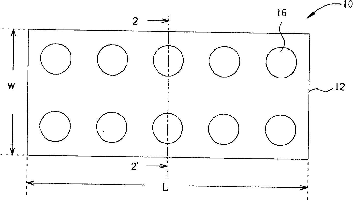
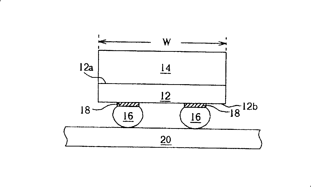
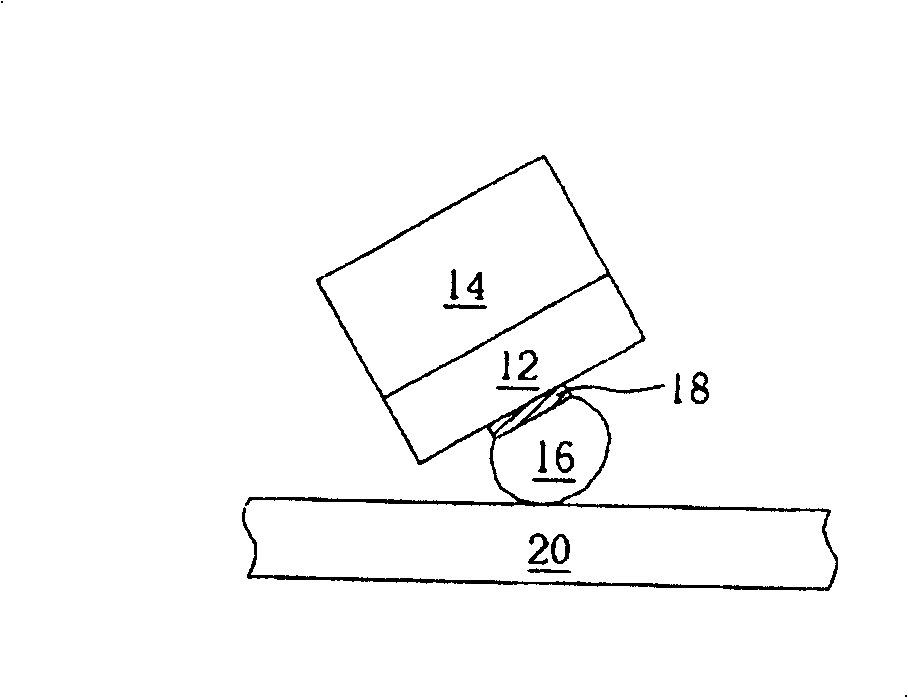
[0030] Please refer to Figure 4 to Figure 6 , Figure 4 It is a bottom view of the semiconductor package structure of the first embodiment of the present invention, Figure 5 for Figure 4 The schematic cross-sectional view of the semiconductor package structure shown along the tangent line 5-5', while Image 6 for Figure 4 The schematic cross-sectional view of the semiconductor package structure shown along the line 6-6'. Such as Figure 4 and Figure 5 As shown, a semiconductor package structure 30 includes a substrate 32 having an upper surface 32a and a lower surface 32b, a chip 34 is disposed on the upper surface 32a of the substrate, a plurality of solder pads 38 are disposed on the lower surface 32b of the substrate 32, and A plurality of bonding balls (bonding balls) 36 are respectively disposed on the surface of each bonding pad 38 . Wherein, the chip 34 is an image sensor chip, such as a CMOS image sensor device or a charge-coupled device, and the chip 34 ca...


PUM


Abstract

The semiconductor package structure on the first base comprises: a second base with first and second surfaces, a chip on first surface, a plurality of first solder balls on second surface and arranged in first direction, and at least one dummy solder block on second surface to avoid the incline of the structure. Wherein, connecting both first solder balls and dummy block to first base.

Description

technical field [0001] The present invention relates to a semiconductor packaging structure, in particular to a ball grid array (BGA) packaging structure with a single row of solder balls. Background technique [0002] Generally speaking, integrated circuit (IC) packages can be divided into pinthrough hole (PTH) and surface mount technology (SMT). Since SMT meets the requirements of high I / O count and high heat dissipation And package size reduction and other requirements, so SMT has become the mainstream of IC packaging technology. In addition, SMT mainly includes ball grid array package (ball grid array, BGA) and chip scale package (chip scale package, CSP). ), and the chip package can be considered as a very small ball grid array package. [0003] Please refer to figure 1 and figure 2 , figure 1 is a bottom view of an existing semiconductor package structure, figure 2 for figure 1 The schematic cross-sectional view of the semiconductor package structure shown alo...

Claims


Application Information

Patent Timeline
Patent Type & Authority Patents(China)
IPC IPC(8): H01L23/48H01L21/60
CPCH01L24/11H01L2224/11H01L2924/14H01L2924/00H01L2924/00012
Inventor 林敏哲
Owner POWERCHIP SEMICON CORP
Why Eureka
Try Eureka