Check patentability & draft patents in minutes with Patsnap Eureka AI!

Semiconductor chip resin encapsulation method

A technology of resin encapsulation and semiconductor, which is applied in semiconductor devices, semiconductor/solid-state device manufacturing, semiconductor/solid-state device components, etc. It can solve the problems that it is not easy to fully fill the resin in the space, the thickness of the packaging resin is small, and the CSP is small.

Active Publication Date: 2009-06-03
DISCO CORP
View PDF5 Cites 0 Cited by
  • Summary
  • Abstract
  • Description
  • Claims
  • Application Information

AI Technical Summary

Problems solved by technology

[0003] This conventional method of encapsulating a semiconductor chip in a resin has the following problems to be solved: it is desired that the CSP as a final product be as small as possible, and thus the thickness of the encapsulating resin is also desired to be as small as possible
Therefore, it is not easy to sufficiently fill the space in the mold with resin

Method used


Image

  • Semiconductor chip resin encapsulation method
  • Semiconductor chip resin encapsulation method
  • Semiconductor chip resin encapsulation method

Examples


Embodiment Construction

[0021] A preferred embodiment of the semiconductor chip resin packaging method according to the present invention will now be described in more detail with reference to the accompanying drawings.

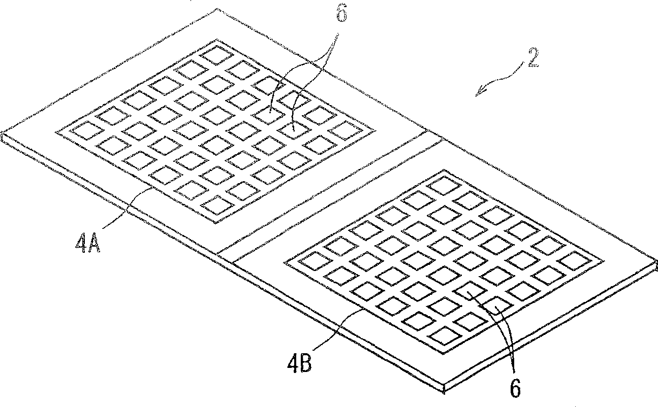
[0022] figure 1 A substrate 2 is shown. The substrate 2 shown is generally in the shape of a rectangular plate and defines two rectangular regions 4A and 4B on the surface of the substrate. A plurality of (36 in the illustrated embodiment) mounting areas 6 are arranged in parallel in a matrix in each of the rectangular areas 4A and 4B. Required electrodes and wires (not shown) are arranged in each rectangular mounting area 6 .

[0023] combine figure 1 further reference figure 2 , a semiconductor chip 8 is bonded to each mounting area 6 placed on the substrate 2 . In more detail, a semiconductor chip 8 is fixed to each mounting area 6 by a suitable fixing means (not shown) such as an adhesive. The electrodes of the semiconductor chip 8 and the electrodes of the mounting area ...


PUM


Abstract

A semiconductor chip resin encapsulation method, including a resin filling and curing step of encapsulating a plurality of semiconductor chips, which have been bonded onto a substrate, in a molten resin, and curing the molten resin. The semiconductor chip resin encapsulation method further includes a grinding step of grinding an upper surface of the cured resin to decrease the thickness of the encapsulating resin to a predetermined value.

Description

technical field [0001] The present invention relates to a semiconductor chip resin encapsulation method for encapsulating a plurality of semiconductor chips which have been bonded to a substrate in a resin. Background technique [0002] Recently, as disclosed in Japanese Patent Application Laid-Open No. 2000-12745, semiconductor devices called CSP (Chip Scale Package) are widely used. To manufacture a CSP, a plurality of semiconductor chips are bonded to a substrate, and these semiconductor chips are encapsulated in resin. The workpiece thus formed is called a CSP substrate. The CSP substrate is then separated at locations between adjacent semiconductor chips. In this way, a plurality of CSPs are manufactured. When encapsulating a plurality of semiconductor chips bonded to a substrate in resin, the plurality of semiconductor chips are usually covered on the substrate with a box-shaped mold having an open lower surface, molten resin is filled into the space in the mold, an...

Claims


Application Information

Patent Timeline
Patent Type & Authority Patents(China)
IPC IPC(8): H01L21/56
CPCH01L24/97H01L23/3121H01L2224/48137H01L21/56H01L24/48H01L21/561H01L2224/97H01L2924/01002H01L2224/16H01L2924/01033H01L2224/32145H01L2924/01006H01L2224/48091H01L2924/01013H01L21/565H01L2924/181H01L2924/00014H01L2924/00011H01L2224/85H01L2924/00012H01L2224/0401H01L2224/45099H01L2224/45015H01L2924/207H01L23/28
Inventor 上野慎治川合章仁
Owner DISCO CORP
Features
  • R&D
  • Intellectual Property
  • Life Sciences
  • Materials
  • Tech Scout
  • Unparalleled Data Quality
  • Higher Quality Content
  • 60% Fewer Hallucinations
Learn More