Chip having high sensitivity for silicon micro-capacitor microphone and preparation method thereof
A condenser microphone, high-sensitivity technology, used in sensors, electrical components, etc., can solve the problems of decreased sensitivity and aging cracks of microphones, and achieve the effects of avoiding aging cracking, reducing corrosion, and avoiding aging cracking.
- Summary
- Abstract
- Description
- Claims
- Application Information
AI Technical Summary
Problems solved by technology
Method used
Image
Examples
Embodiment 1
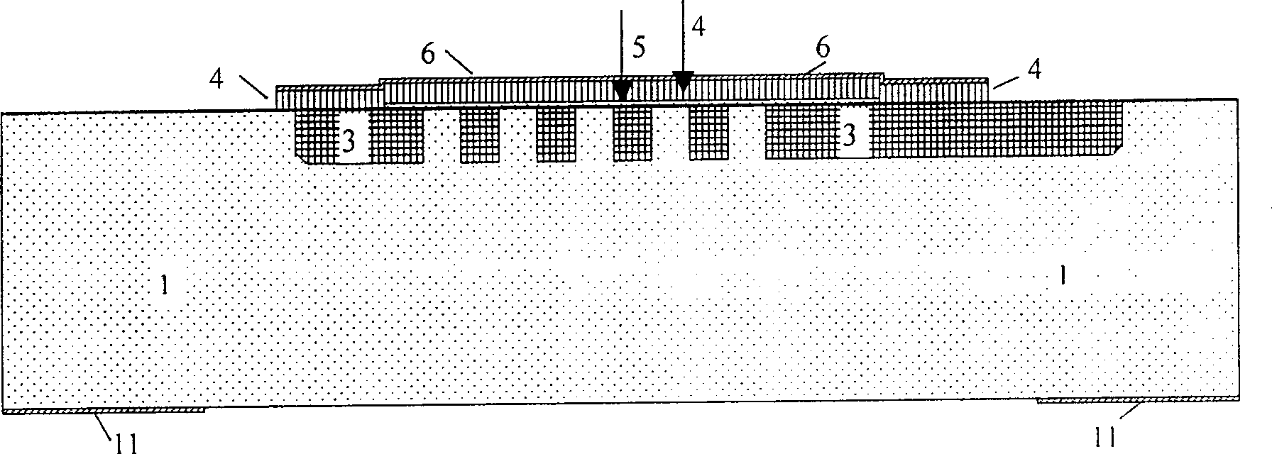
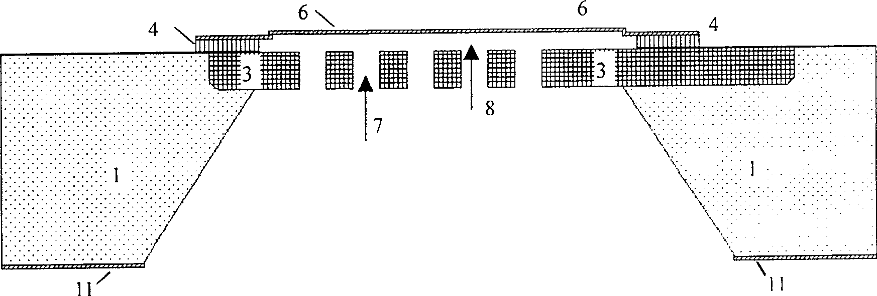
[0038] A kind of chip of the present invention that this embodiment provides is used in silicon microcapacitance microphone, see appendix Figure 4 —6; This chip comprises an n-type silicon substrate 1, forms p+ type doped layer 3 at the front of silicon substrate 1 diffused boron, and its thickness is 3 or 20 microns; Deposits silicon dioxide at p+ type doped layer 3 and Photoetching and etching into an annular isolation layer 4, the inner diameter of the annular isolation layer 4 is 500 or 3000 microns, and the radial width is 50 or 150 microns; Shaped vibrating membrane layer 6, deposited on the vibrating membrane layer 6 and photoetched, corroded into a circular metal aluminum film and a square electrode 9, uniform circular micro-perforations 10 are distributed on the edges of the vibrating membrane and the circular aluminum film; The circular micro-perforation 10 has a diameter of 1-20 microns; its center is located on a concentric circle with a diameter of 70-98% of the d...
Embodiment 2
[0040] combined with Figure 7 The preparation method of the present invention is described in detail with specific examples:
[0041] [1] Take an n-type silicon substrate 1 and grow a silicon dioxide with a thickness of 1.5 microns through high-temperature oxidation. After photolithography, use hydrofluoric acid to etch the high-temperature silicon dioxide to make a mask 2, and place it Carry out deep boron diffusion to form the p+ type doped layer 3 in the perforated backplane except for the hole distribution part, and the boron diffusion depth is 10 microns;
[0042] [2] After removing the high-temperature silicon dioxide mask with hydrofluoric acid, a 0.5-micron-thick zinc oxide auxiliary sacrificial layer is magnetron sputtered on the front of the silicon wafer, and a circular auxiliary sacrificial layer 5 is formed by photolithography and phosphoric acid etching. The diameter of the auxiliary sacrificial layer is 1000 microns, and the thickness is 0.5 microns; on the fr...
PUM
| Property | Measurement | Unit |
|---|---|---|
| thickness | aaaaa | aaaaa |
| width | aaaaa | aaaaa |
| diameter | aaaaa | aaaaa |
Abstract
Description
Claims
Application Information


