Transistor structure with breakdown protection

A technology of breakdown protection and transistors, applied in the direction of transistors, semiconductor devices, electrical components, etc., can solve problems such as inconvenience

Inactive Publication Date: 2009-07-15
SYST GEN
View PDF7 Cites 0 Cited by
  • Summary
  • Abstract
  • Description
  • Claims
  • Application Information

AI Technical Summary

Problems solved by technology

However, due to the deviation of the process itself, generally speaking, the range of ion doping concentrations that can achieve a higher avalanche breakdown voltage is not large, resulting in different breakdown voltages for components produced by the same process
[0008] Therefore, it can be seen from the above that the above-mentioned known transistor structure with breakdown protection obviously has inconvenience and shortcomings in actual use.

Method used


Image

  • Transistor structure with breakdown protection
  • Transistor structure with breakdown protection
  • Transistor structure with breakdown protection

Examples


Embodiment Construction

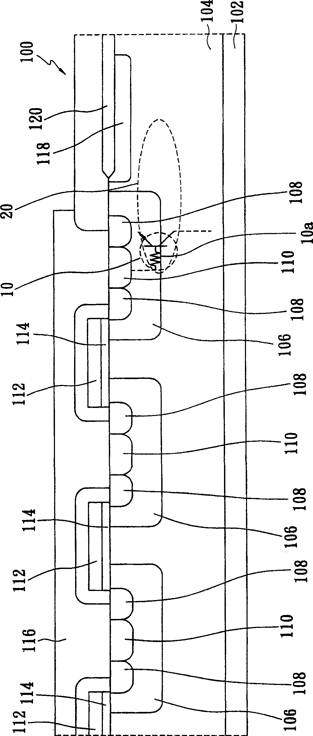
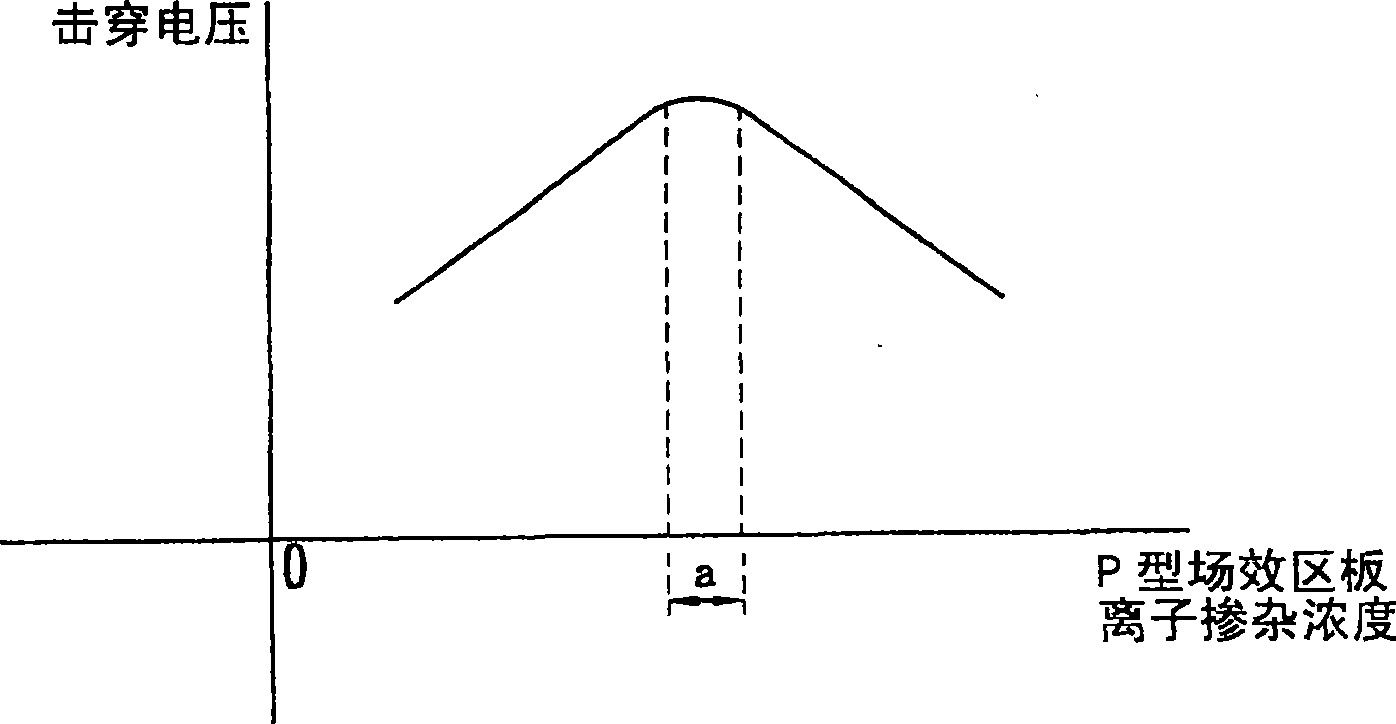
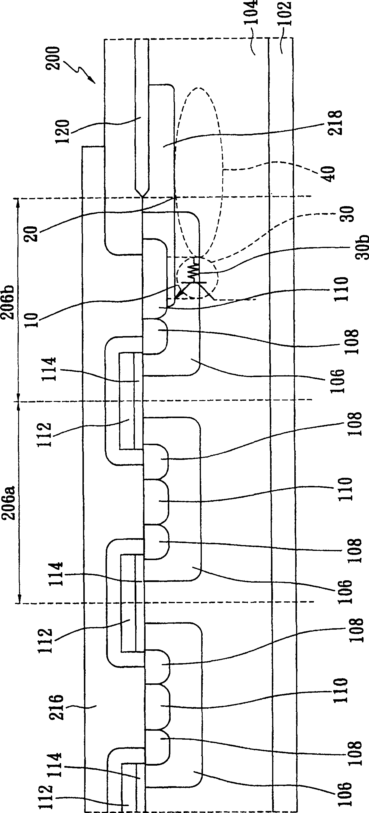
[0052] Such as figure 2 Shown is a partial cross-sectional view of an embodiment of the transistor structure with breakdown protection of the present invention. In this vertical Depletion MOS (DMOS) 200, it includes at least one transistor module (module) 206a, a surrounding transistor module 206b, and a P-field effect block (P-field). block) 218, and a metal field effect block 216 extending above the P-type field effect block 218.

[0053] The transistor module 206b mainly includes an N-type heavily doped region (first-type ion heavily doped region) 108, a P-type heavily doped region (second-type ion heavily doped region) 110, and a P-type well Area (second-type ion doping region) 106, part of the N-type layer 104, and part of the P-type field effect block (second-type ion doping field effect block) 218, in addition to an N+ substrate 102, a gate The electrode 112, and a gate oxide layer 114. At the same time, because the transistor module 206b is located in the N-type layer (fi...


PUM


Abstract

The invention relates to a transistor structure with breakdown protection, which can improve the withstand breakdown energy of the transistor and expand the redundancy of ion doping concentration required by the predetermined avalanche breakdown voltage. The transistor structure prevents the parasitic bipolar transistor from being turned on, and can improve the avalanche breakdown resistance current of the transistor. At the same time, the transistor structure has a metal field effect block, which is used to expand the redundancy of the ion doping concentration required for the predetermined avalanche breakdown voltage.

Description

Technical field [0001] The invention relates to a transistor structure with breakdown protection. Background technique [0002] Single-Shot Avalanche Breakdown Energy (Single-Shot Avalanche Breakdown Energy, E AS ) Is one of the factors to evaluate the characteristics of a transistor. It represents the energy that the transistor can withstand when a single avalanche breakdown (Avalanche Breakdown) occurs. When this energy is exceeded, the junction temperature of the transistor will be too high. Cause internal damage to the component. General estimate E AS The formula is: [0003] E AS =V BR *I AS *T AS [0004] Where V BR Is the transistor breakdown voltage, I AS Is the avalanche breakdown current, and T AS Is the avalanche breakdown time. [0005] Such as Figure 1A Shown is a partial cross-sectional view of a known transistor 100 having a P-field plate 118, in which an N-type layer 104 (N-epi), a P-type well region 106, and a The N-type heavily doped region 108 and a P-type he...

Claims


Application Information

Patent Timeline
Patent Type & Authority Patents(China)
IPC IPC(8): H01L29/72H01L29/772
Inventor 黄志丰简铎欣蒋秋志
Owner SYST GEN
Why Eureka
Try Eureka