Transistor structure with breakdown protection
A technology of breakdown protection and transistors, applied in the direction of transistors, semiconductor devices, electrical components, etc., can solve problems such as inconvenience
- Summary
- Abstract
- Description
- Claims
- Application Information
AI Technical Summary
Problems solved by technology
Method used
Image
Examples
Embodiment Construction
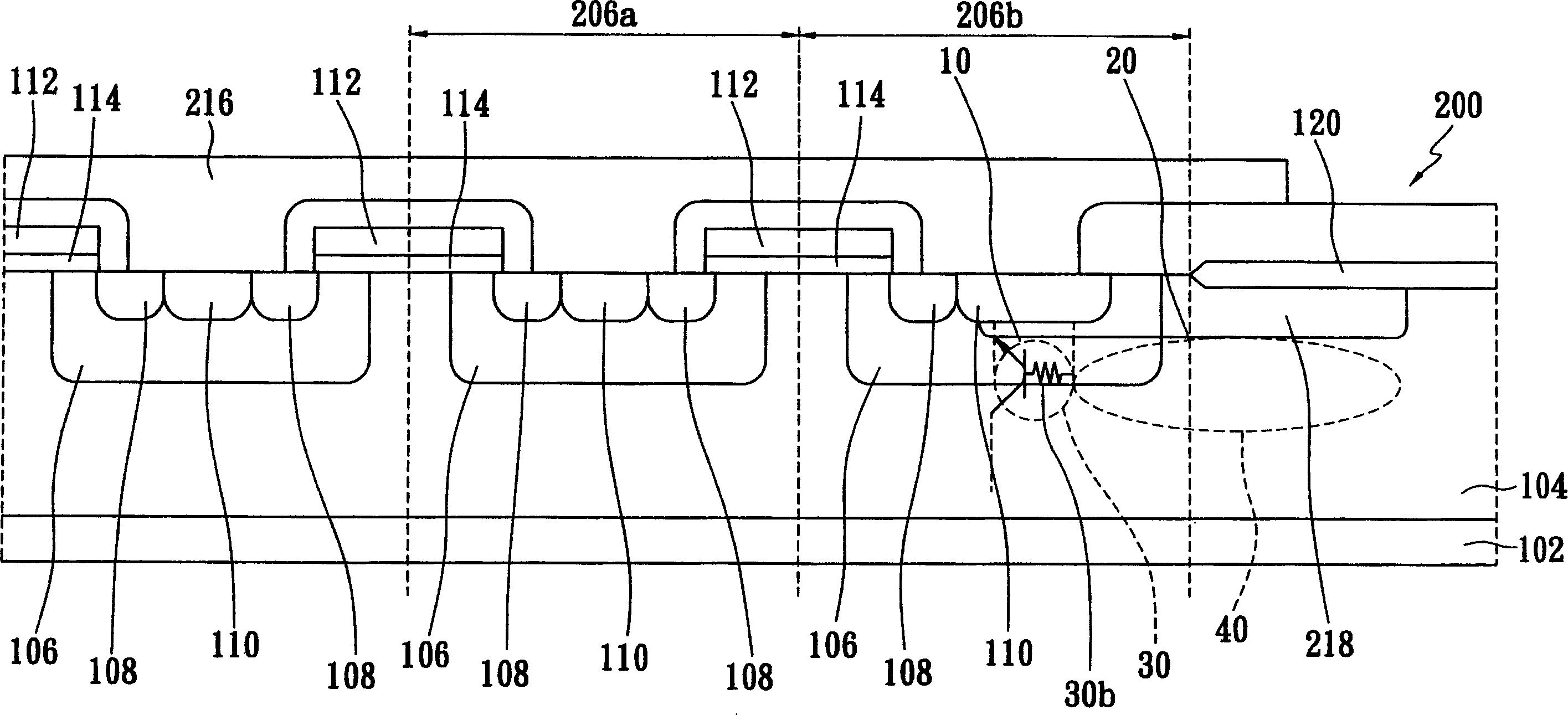
[0052] like figure 2 Shown is a partial cross-sectional view of an embodiment of the transistor structure with breakdown protection of the present invention. In this vertical Depletion MOS (depletion-type metal oxide semiconductor transistor, DMOS) 200, including at least one transistor module (module) 206a, a transistor module 206b located around, a P-type field effect block (P-field block) 218, and a metal field effect block 216 extending above the P-type field effect block 218.
[0053] The transistor module 206b mainly includes an N-type heavily doped region (first type ion heavily doped region) 108, a P type heavily doped region (second type ion heavily doped region) 110, a P type well Region (second-type ion-doped region) 106, part of N-type layer 104, and part of P-type field effect block (second-type ion-doped field effect block) 218, and also includes an N+ substrate 102, a gate electrode 112, and a gate oxide layer 114. At the same time, because the transistor mo...
PUM
 Abstract
Description
Claims
Application Information


