4h-sic ultraviolet photodetector with double working mode and preparation method thereof

A double-working mode, electrical detector technology, applied in the direction of circuits, electrical components, semiconductor devices, etc., can solve the problems of low UV/visible suppression ratio, high doping concentration of multiplication layer, high avalanche breakdown voltage, etc., and achieve high UV / Visible suppression ratio, low avalanche breakdown voltage, low dark current effect

Active Publication Date: 2017-10-03
XIAMEN UNIV
View PDF3 Cites 0 Cited by
  • Summary
  • Abstract
  • Description
  • Claims
  • Application Information

AI Technical Summary

Problems solved by technology

SiC ultraviolet photodetectors with PIN structure are generally used for high-speed and simple detection of optical signals, and have the advantages of fast response speed, low dark current and low power consumption. It will be completely exhausted when working at working voltage or zero bias; however, its avalanche breakdown voltage is high, the power consumption of the device is large, and there is no internal gain, so it cannot work stably in the state of avalanche breakdown voltage
SiCAPD with SAM structure is generally used in the detection of weak ultraviolet signals and single photon signals. The separation of the absorption layer and the multiplication layer in the punch-through state can reduce the breakdown voltage of the device, and has the advantages of small avalanche noise and large internal gain; however, its multiplication The layer doping concentration is relatively high, resulting in a large dark current, and in the low-voltage working state, the active region of the device cannot be completely depleted, resulting in low spectral response, low UV / Vis suppression ratio, and performance far lower than PIN photodetectors

Method used


Image

  • 4h-sic ultraviolet photodetector with double working mode and preparation method thereof
  • 4h-sic ultraviolet photodetector with double working mode and preparation method thereof
  • 4h-sic ultraviolet photodetector with double working mode and preparation method thereof

Examples


Embodiment Construction

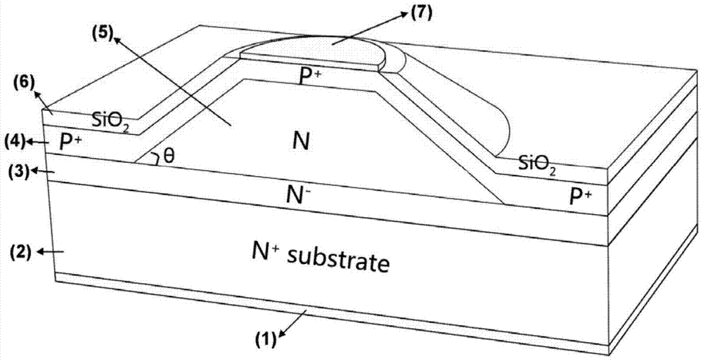
[0032] Such as figure 1 As shown, the 4H-SiC ultraviolet photodetector embodiment of the double working mode of the present invention is provided with N + Type 4H-SiC substrate 2, in N + Type 4H-SiC substrate 2 is sequentially provided with first N - Type epitaxial absorption layer 3 and the second N-type epitaxial multiplication layer 5; from the second N-type epitaxial multiplication layer 5 to the first N - The surface of the epitaxial absorption layer 3 is etched to a height so that the second N-type epitaxial multiplication layer 5 is a cone; - P + type ohmic contact layer, forming a P + N and P + N - Two PN junctions; at P + A silicon dioxide layer is grown on the surface of the type ohmic contact layer as the passivation layer of the device; a P-type electrode window is arranged on the passivation layer, and a P-type electrode window and an N + Type 4H-SiC substrate 2 is sputtered on the back of P electrode and N electrode respectively.

[0033] The first N - ...


PUM


Abstract

The invention relates to a 4H-SiC ultraviolet photoelectric detector in double work modes, a manufacturing method thereof and a semiconductor photoelectric detector device. The detector is provided with an N+-type 4H-SiC substrate, and a first N-type epitaxial absorbed layer and a second N-type epitaxial multiplication layer are sequentially arranged on the N+-type 4H-SiC substrate; surface etching to a certain height from the second N-type epitaxial multiplication layer to the first N-type epitaxial absorbed layer is carried out; a P+-type ohmic contact layer is formed at surfaces of the second N-type epitaxial multiplication layer and the surface of the first N-type epitaxial absorbed layer, and two P+N knots are formed; a silica passivation layer is grown on the surface of the P+-type ohmic contact layer; a P-type electrode window is formed on the passivation layer, and a P electrode and an N electrode are respectively sputtered in the P-type electrode window and the back face of the N+-type 4H-SiC substrate. The manufacturing method comprises steps that, RCA standard cleaning for a well-grown epitaxial wafer is carried out; an inclination table board is manufactured; the P+ layer is manufactured; an oxidation layer is manufactured; the electrode is manufactured.

Description

technical field [0001] The invention relates to a semiconductor photodetection device, in particular to a 4H-SiC ultraviolet photodetector with a detection wavelength of 200-400nm and a double working mode and a preparation method thereof. Background technique [0002] Ultraviolet photodetectors can be widely used in military and civilian fields, such as missile early warning, rocket launch, and aircraft guidance in military applications, and in biomedical analysis, fire alarm, and solar ultraviolet intensity measurement in civilian applications. , so it has broad application prospects and is one of the frontier research directions in the field of photodetection. 4H-SiC is one of the core materials of the third-generation wide bandgap semiconductor. It has the advantages of high critical breakdown electric field, high saturation electron velocity, high electron mobility and high thermal conductivity, and has become a popular material for the preparation of high-performance u...

Claims


Application Information

Patent Timeline
Patent Type & Authority Patents(China)
IPC IPC(8): H01L31/11H01L31/0352
CPCH01L31/035281H01L31/11
Inventor 洪荣墩张明昆吴正云蔡加法陈厦平
Owner XIAMEN UNIV
Why Eureka
Try Eureka