Method for producing substrates

A substrate and deviation technology, applied in multilayer circuit manufacturing, printed circuit manufacturing, printed circuit components, etc., can solve problems such as circuit board defects, different deformation characteristics, and insufficient overlapping of connection surfaces

Inactive Publication Date: 2009-07-22
HITACHI SEIKO LTD
View PDF6 Cites 0 Cited by
  • Summary
  • Abstract
  • Description
  • Claims
  • Application Information

AI Technical Summary

Problems solved by technology

[0009] However, different layers often exhibit different deformation characteristics, or later layers cannot track specific deformations of underlying layers due to technological process aspects
In this case, when using the transformation described by Equation 1, the connection faces of the different printed conductor structures are usually arranged offset from each other, so that the overlap between the connection faces to be bonded is often not large enough to achieve the corresponding connection faces reliable electrical connection
Therefore, boards manufactured in this manner are often defective and must be sorted out of the manufacturing process

Method used


Image

  • Method for producing substrates
  • Method for producing substrates
  • Method for producing substrates

Examples


Embodiment Construction

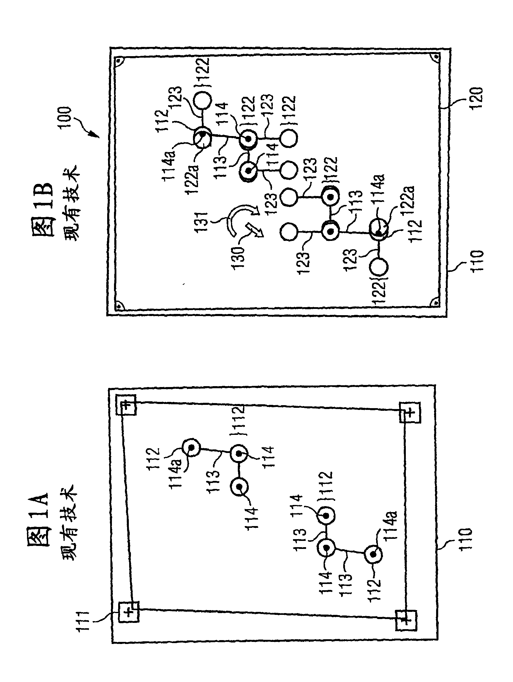
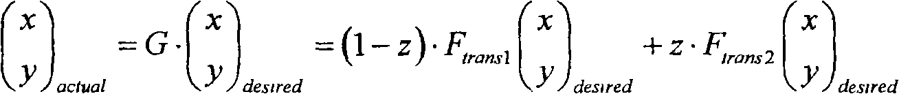
[0027] Figures 1a and 1b illustrate the manufacture of a circuit board 100 structured in layers according to the prior art. The construction of the circuit board 100 begins with a first layer 110 with four markings 111 applied thereto. The positions of these markers are measured and a transformation according to Equation 1 is determined from the deviation between the actual position and the respective ideal position, by means of which transformation the deformation of all grid points of the first layer 110 is determined. Usually, this deformation can be easily obtained for all grid points.

[0028] According to the presently shown embodiment, the printed wire structure formed on the first layer 110 includes a total of six first connection surfaces 112, and these six connection surfaces are divided into two groups, and each group includes three first connection surfaces 112 . The connection areas 112 in each of the two groups are connected via two first conductor tracks 113 ....


PUM


Abstract

The invention provides a method for the manufacture of a substrate (200), wherein the substrate is manufactured by successive two-dimensional process steps so as to comprise a first layer (210) and at least one second layer (220) adapted to the first layer ). First, several marks (211) are measured on the first layer (210), and the deviation of the actual position of each mark (211) from the ideal position is determined. From these deviations, a transformation Ftrans1 of positional deviations of any grid point of the first layer (210) is determined, and a transformation Ftrans2 of possible positional deviations of grid points of the second layer (220) is determined. When determining the transformation Ftrans2, the previously known constraints on the possible deformation states of the second layer are taken into account. During the subsequent processing of the second layer ( 220 ), the combined transformation of the two previously determined transformations Ftrans1 and Ftrans2 is taken into account. Thus, even if the two layers 210, 220 have different deformations, a reliable connection of the circuit can be ensured, so that during the manufacture of the multilayer circuit board less defective circuit board rejects are produced.

Description

technical field [0001] The invention relates to a method for producing a multilayer substrate, wherein the multilayer substrate is produced with a first layer and at least one second layer matched to the first layer by successive two-dimensional processing steps. Background technique [0002] During the construction of a multilayer circuit board, the layers of the circuit board are pressed against each other many times. The temperature and compressive stresses applied during this process cause unwanted deformations, such as shrinkage or elongation, in the material used for the circuit board. In different extrusion operations, circuit boards can change their dimensions several times before they are finished. Depending on the layout of the board, ie the structure of the printed conductors realized by the copper surface in a single layer, non-linear deformations can also occur, where elongation or contraction in different directions results in different intensities. [0003] ...

Claims


Application Information

Patent Timeline
Patent Type & Authority Patents(China)
IPC IPC(8): H05K3/46H05K1/02H05K3/00
CPCH05K3/4644H05K3/4679H05K1/0269H05K2201/09918H05K3/0035
Inventor 托马斯·奎克乌韦·梅特卡罗兰德·施蒂策
Owner HITACHI SEIKO LTD
Why Eureka
Try Eureka